Wide-Bandgap Semiconductors Explained in One Sitting
Wide bandgap semiconductors explained: the band gap decides how much voltage a material holds, how hot it runs and what colour light it emits.
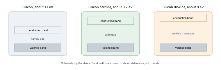
Every material used to make a semiconductor device can be described by one number: the energy an electron must gain to break free of the atomic lattice and start conducting. That number, the band gap, predicts how much voltage the material can hold, how much current it leaks when hot, and even what colour light a device made from it emits.
Last updated:
Energy bands without equations
In a solid, electrons cannot take just any energy value. They occupy bands. The lower band, called the valence band, holds electrons that are still bound to atoms. The upper band, the conduction band, holds electrons free enough to move and carry current. Between them sits a range of energies that no electron may occupy, which is why the gap has a second name: the forbidden energy gap.
The analogy that works for a beginner is a set of shelves with a missing shelf. Electrons can sit on the lower shelf or the upper shelf, and there is a height they must be lifted through to get from one to the other. The band gap is that height. It is measured in electronvolts — the energy one electron gains when it crosses a potential difference of one volt — and it is a property of the material rather than of any particular device.
What “bandgap” decides
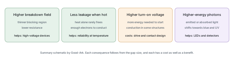
Four practical properties follow from the size of the gap. First, the breakdown field: a wider gap means the material can withstand a stronger electric field before it starts conducting when it should not, which is what allows a low-loss high-voltage device. Second, leakage at temperature: a wider gap makes it much harder for heat alone to free electrons, so the device leaks less when hot. Third, the threshold voltage of a forward-conducting device, which rises with the gap. Fourth, the light a device can emit or absorb, because the photon energy has to match the gap.
That fourth point is why the same concept explains two industries that look unrelated. Visible light spans roughly 1.8 to 3.1 electronvolts, so a material with a gap in that range can emit visible light — which is exactly why the materials used in LEDs have gaps chosen for the colour they produce.
| Material | Approximate band gap | Where you meet it |
|---|---|---|
| Germanium | about 0.7 eV | The first widely used transistor material, now specialised uses |
| Silicon | about 1.1 eV | Almost all logic, and the majority of power devices |
| Gallium arsenide | about 1.4 eV | High-frequency and optoelectronic devices |
| Silicon carbide (4H) | about 3.2 eV | High-voltage power conversion |
| Gallium nitride | about 3.4 eV | Compact power supplies, radio frequency, LEDs |
| Diamond | about 5.5 eV | Research and specialised devices, not main stream |
| Silicon dioxide | about 9 eV | An insulator, not a semiconductor — which is why it is used to isolate |
Why silicon ran out of headroom
Silicon’s gap of about 1.1 electronvolts is a good compromise, which is why it dominates. It is wide enough to make a stable transistor and narrow enough that the devices switch at modest voltages. But for high-voltage power conversion, the compromise shows. To block a kilovolt, a silicon device needs a thick, lightly doped region, and thicker material means more resistance and more waste heat.
The limit is not a manufacturing problem that better engineering will remove; it is a property of the material. That is why, after decades of squeezing silicon, the industry looked sideways at materials with wider gaps rather than continuing to refine the same one.
The two challengers
Two materials with wider gaps have reached commercial scale in power electronics. Silicon carbide, at roughly 3.2 electronvolts, is used where the voltage is high: solar inverters, vehicle traction systems, industrial drives. Gallium nitride, at roughly 3.4, is used where the frequency is high and the voltage moderate: compact chargers, server supplies, radio-frequency devices.
The split is not arbitrary and it is not about the band gap, which the two share almost exactly. It follows from how each material is built into a device. Silicon carbide is commonly made as a vertical device, with current flowing through the thickness of the die, which scales naturally to high voltage. Gallium nitride is commonly made as a lateral device, with current flowing along the surface, which suits high frequency and moderate voltage. Same physics, different geometry, different market.
Everyday products affected
The clearest everyday example is the small gallium nitride charger, which exists because higher switching frequency allows smaller magnetics. The second is the electric vehicle, where wide-bandgap devices reduce losses in the conversion stages and allow smaller, lighter power electronics. The third is rooftop solar, where the inverter runs daily for years and efficiency accumulates. The fourth is the LED, which is an optoelectronic device whose colour is set by a band gap, although the materials are different from the ones used for power switching.
What none of these have in common is that wide-bandgap devices took over the product. In every case they occupy the positions where voltage, frequency or duty cycle justify them, and conventional silicon stays in the rest of the design.
What this means for costs and standards
Cost follows the material. Silicon carbide wafers are grown slowly at high temperature and are available in smaller diameters than silicon, so the device price carries a substrate premium. Gallium nitride benefits from being buildable on silicon substrates with processes closer to established fabrication, which is why it reached consumer price points faster.
Standards follow the application rather than the material. A wide-bandgap device intended for automotive use is qualified to the same automotive expectations as any other device, and the test methods that make datasheet numbers comparable come from the same bodies. The material changes the physics; it does not create a separate regulatory world. Background written for beginners covers band gap, silicon carbide and gallium nitride, with device test methods published by JEDEC, system expectations from the International Electrotechnical Commission, and sector reporting from the Semiconductor Industry Association. Wide bandgap and sector background is published by the US Department of Energy, NIST and ISO.
Common misunderstandings
Four beliefs are worth correcting. The first is that a wider band gap always means a better device — it also means a higher turn-on voltage and harder contacts, which is why very wide-gap materials remain difficult to commercialise. The second is that wide-bandgap materials are new; silicon carbide has been manufactured industrially since the nineteenth century, and only the single-crystal quality is recent. The third is that they are replacing silicon, which they are not. The fourth is that the band gap is a device rating; it is a material property, and the device’s ratings are several steps removed from it.
One-page summary
The band gap is the energy an electron must gain to move from the valence band to the conduction band, measured in electronvolts. A wider gap means a higher breakdown field, less leakage at temperature, a higher turn-on voltage and higher-energy photons. Silicon sits at about 1.1 electronvolts and dominates electronics; silicon carbide and gallium nitride sit around 3.2 and 3.4 and take the high-voltage and high-frequency niches respectively. Nothing in this subject requires equations to understand — only the shelf picture and the four consequences that follow from it.
FAQ
What do you understand by band gap of semiconductor?
The band gap is the energy difference between the top of the valence band, where electrons are still bound to atoms, and the bottom of the conduction band, where they are free to move and carry current. It is measured in electronvolts and it is a property of the material. For a semiconductor, the gap is small enough that heat, light or an applied voltage can lift electrons across it, which is what makes the material controllable rather than simply insulating.
Which semiconductor has the highest band gap?
It depends on where the boundary of the category is drawn. Among materials routinely used as semiconductors, diamond has the widest gap at roughly 5.5 electronvolts, with aluminium nitride wider still at around 6 and silicon carbide and gallium nitride lower at about 3.2 and 3.4. Beyond that, conventional insulators such as silicon dioxide have gaps near 9 electronvolts. A material with a gap that wide stops behaving as a controllable semiconductor in normal conditions, which is precisely why it is used as an insulator.
What happens if the band gap increases?
Four things follow. The material withstands a higher electric field before breaking down, so devices can block more voltage in less material. It leaks less current at high temperature, because heat alone is less likely to free electrons. It requires a higher voltage to start conducting, which complicates the design of contacts and drive circuits. And any light it emits or absorbs shifts to higher energy, meaning bluer or ultraviolet. Whether that is good depends entirely on which device you are trying to build.
What is the forbidden energy gap?
It is another name for the same thing. The term emphasises that between the valence and conduction bands there is a range of energies that electrons cannot occupy in that material. The forbidden zone is what forces an electron either to stay bound or to gain the full gap energy and become free; there is no halfway state. That discontinuity is the reason semiconductor behaviour is switchable rather than gradual.
Do I need the physics to choose a device?
No, but it helps you avoid one category of mistake. Understanding that a wider gap means a higher breakdown field explains why high-voltage devices come from particular materials, and understanding that it also means a higher turn-on voltage explains why the same materials are awkward at low voltage. For actually selecting a part, the datasheet is the tool; the physics is what tells you which datasheet pages to read. Our guide to silicon carbide applies that reasoning to one material.
What to do next
The useful habit is to translate every material claim into one of the four consequences above, and then ask which one the application cares about. A claim that a material is “wider bandgap” is not an argument for anything on its own. Our guide to silicon carbide versus gallium nitride applies the same translation to the two commercial options.
Tell Good-Ark the blocking voltage, the switching frequency and the thermal budget, and we can point to the device families that fit and explain what the material choice costs you in design effort.
Email sales@goodark.com, or start from the product family learning centre.
This article is published by Good-Ark, a manufacturer of silicon carbide devices. Band gap values are approximate published figures that vary by crystal structure, alloy composition and temperature; they are given here to show magnitudes, not for calculation.
Continue through this engineering topic
For the complete selection, design, verification, and troubleshooting path, explore the Silicon Carbide and Wide Bandgap Hub.
Recommended
 Why Do Diodes Get Hot? Conduction and Switching Losses ExplainedInfoStandard, Fast Recovery, and Schottky Diodes: What’s the Difference?Info
 What Is a Fast Recovery Diode? Understanding “Fast Recovery”Info
 What Is a Diode? A Beginner’s Guide to How It WorksInfo
 Automotive Semiconductor Report 2026: Chips Per Car Keep RisingKnowledge