Low RDS(on) Explained: Why It Decides Your Battery Life
Low RDS(on) explained: on-resistance is the toll a MOSFET charges on every amp. How to read it at the right gate voltage, and when it pays back.
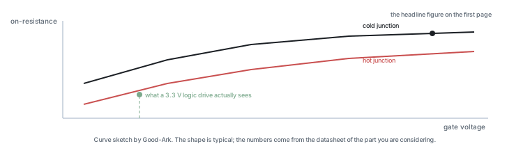
On-resistance is the toll a MOSFET charges on every amp that passes through it, and in a battery-powered product that toll is paid out of the battery. The size of the toll depends on two conditions the datasheet states and that beginners routinely ignore: the gate voltage and the junction temperature.
Battery life is a resistance story
A battery has a fixed amount of energy, and every component in the path between it and the load spends some of it. A switching MOSFET spends energy as heat in proportion to its resistance and the square of the current, so the difference between one device and another becomes a difference in running time.
The analogy that works is a long cable with a slightly undersized conductor. Nothing fails, the equipment runs, and some of the battery’s energy warms the conductor instead of doing work. On a bench with a power supply that difference is invisible; in a device that has to run for a week on one charge it is the difference between a product that meets its specification and one that does not.
What RDS(on) means in one line
RDS(on) is the resistance between drain and source when the device is fully on, and it is the figure that determines conduction loss. Multiply it by the square of the current and you have the power turned into heat. The symbol appears in datasheets as RDS(on) because it is a resistance between the drain and the source measured in the on state, and the “on” in brackets is the part that matters: it is a different number at every gate voltage.
Two conditions must therefore accompany the figure for it to be useful: the gate voltage at which it was measured, and the junction temperature. A datasheet that lists one number without either has given you the best case rather than the operating case.
Why the datasheet number changes with temperature
On-resistance rises with junction temperature, and for silicon devices the room-temperature figure is roughly the lowest the part will ever present. Datasheets therefore include a normalised curve showing the multiplier against temperature, and the useful number is the base figure multiplied by the value on that curve at your operating temperature.
The effect is not small. Across the common range, the multiplier can approach two, which means a design estimated from the room-temperature number can be dissipating nearly twice the heat it was sized for. That is why thermal estimates use the hot figure and why the practice of checking a design with a finger on a cool device on a bench proves nothing about its behaviour in a warm enclosure.
A 10 A example you can follow
The numbers below are invented round figures chosen to make the arithmetic visible. They are not a specification for any part, and real devices vary widely.
| Step | Part A | Part B |
|---|---|---|
| On-resistance at the gate voltage used, cold | 10 milliohms | 5 milliohms |
| Multiplier at the operating temperature | 1.6 | 1.6 |
| On-resistance hot | 16 milliohms | 8 milliohms |
| Conduction loss at 10 A | 1.6 W | 0.8 W |
| Heat saved by choosing part B | 0.8 W, continuously, whenever the load is on | |
| Consequence in a battery product | Less energy wasted, lower temperature, or a smaller thermal design | |
The final row is where the decision lives. Half a watt per switch sounds small until you multiply it by hours of operation and by the number of switches in the product, and until you remember that the heat has to be removed from a sealed enclosure. In a battery-powered device running for eight hours at a time, that difference can be a measurable fraction of the total energy budget.
When low RDS(on) is worth paying for
Three situations justify the premium. The device carries high current for a large fraction of the time, so the loss accumulates. The thermal budget is tight, so removing heat is more valuable than the component cost. Or the product runs on a battery, where the loss comes directly out of running time that the customer can measure.
There are also situations where it is not worth paying for. A device that switches briefly and carries little current spends most of its life in the off state, where its on-resistance is irrelevant. A circuit with a generous thermal path and mains power has no reason to care about half a watt. And a design operating at a gate voltage below the one used for the low-resistance figure will not achieve that figure anyway, so the premium buys nothing.
What else steals your battery
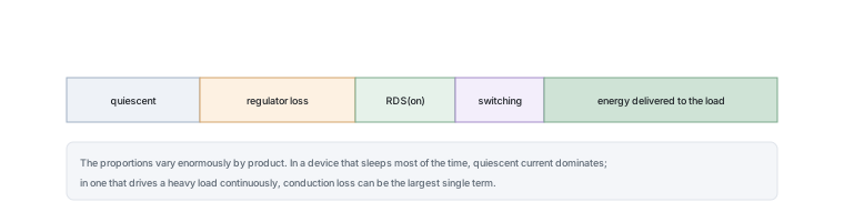
On-resistance is one term in a longer list. Quiescent current — what the circuit draws while idle — is often the dominant loss in a device that spends most of its time waiting. Switching losses in the converter, the efficiency of the regulator, the leakage in capacitors and the self-discharge of the battery itself all take their share. A design that optimises on-resistance while leaving a regulator running at poor efficiency has improved the smallest term in the sum.
The practical consequence is to look at the whole energy budget before paying for one component. A short list of where the energy goes usually shows which improvement has the largest effect, and on-resistance is only the answer when the load current is high and the duty cycle is long.
How to compare two parts fairly
Comparison requires the same conditions on both sides. Read the on-resistance at the gate voltage your circuit provides and at the junction temperature it will reach, on both candidates, and only then compare. If one datasheet quotes at a higher gate voltage than the other, the comparison is meaningless until you find the matching curve.
Four further checks belong in the same exercise. The total gate charge, because a device with lower on-resistance but a much larger gate charge can lose more energy switching than it saves conducting. The thermal resistance, because a lower-loss part in a package that cannot shed heat is not an improvement. The package, because it determines how much copper you can give it. And the blocking voltage, since a part with a higher voltage rating usually has a higher on-resistance for the same die area.
There is also a version of this argument that has nothing to do with the datasheet, and it is worth stating because it changes what people buy. The energy a device saves is only relevant if the device is in the conducting path for a meaningful fraction of the product’s operating time. In a product that spends most of its life asleep, or in a switch that operates for a few seconds an hour, the saving is real but negligible, and paying a premium for it is a choice rather than an optimisation.
Takeaways
On-resistance is a condition-dependent number, and the conditions that matter are your gate voltage and your operating temperature. Conduction loss is the square of the current multiplied by that figure, and in a battery product it comes out of running time. Lower is better when the device carries significant current for a significant fraction of the time, and irrelevant when it does not.
Our own articles cover MOSFET and power MOSFET. Device test methods come from JEDEC, thermal and assembly expectations from IPC, and sector-level context from the Semiconductor Industry Association. Device and quality background is published by ISO, NIST and IEC.
FAQ
What is RDS(on) in a MOSFET?
It is the resistance between the drain and source terminals when the device is fully on. Multiplying it by the square of the current gives the conduction loss. It is not a fixed property of the part: it depends on the gate voltage applied and on the junction temperature, which is why a datasheet lists it at stated conditions and includes a curve showing how it rises with heat.
What do drive voltage, maximum RDS(on) and minimum RDS(on) mean?
The drive voltage is the gate voltage the figure is quoted at, and it is the condition that decides which number applies to your circuit. A maximum figure is the guaranteed worst case across production and temperature, and it is the number a design should be checked against. A minimum figure is the best case, useful for understanding the spread but not for design. Where a datasheet gives one headline number without either condition, treat it as a typical value at a favourable condition rather than as a guarantee.
How do I calculate the RDS(on) of a MOSFET?
You do not calculate it, because it is a measured property. What you calculate is the loss it causes: take the on-resistance at your gate voltage, multiply by the temperature multiplier from the datasheet curve, then multiply by the square of your current to get watts. That figure is what the thermal design has to remove, and dividing the resulting temperature rise by your allowance tells you whether the part is suitable.
What kills MOSFETs?
Gate overvoltage, overheating, avalanche events beyond the rating, and shoot-through in bridge circuits. In this context the relevant point is that running a device hotter than intended accelerates every one of those mechanisms, because higher temperature raises on-resistance, which raises the current density and the stress on the internal connections. The general treatment is in our article on what a MOSFET is.
Is a lower RDS(on) always better?
Not always. Lower on-resistance usually comes with a larger die, a higher gate charge and a higher price, and none of those is free. A device that conducts briefly at low current gains nothing from a low on-resistance, and one driving a gate with limited current can lose more in switching than it saves in conduction. Choose it when the current and the duty cycle make conduction loss a significant term.
What to do next
Take a battery-powered device you own and work out roughly where its energy goes: idle current, regulator losses, conduction and switching. The proportion that turns out to dominate is the one worth improving, and it is not always the one the catalogue highlights. Our article on why MOSFETs get hot covers the thermal side of the same calculation.
Give Good-Ark the current, the duty cycle, the gate voltage and the ambient temperature, and we can compare the two on the same conditions and tell you whether the difference pays for itself.
Email sales@goodark.com, or start from the product family learning centre.
This article is published by Good-Ark, a manufacturer of MOSFETs and other discrete devices. The example figures are invented round numbers used to show the arithmetic; on-resistance and its temperature behaviour belong to the current official datasheet of the part.
Recommended
 Why Do Diodes Get Hot? Conduction and Switching Losses ExplainedInfoStandard, Fast Recovery, and Schottky Diodes: What’s the Difference?Info
 What Is a Fast Recovery Diode? Understanding “Fast Recovery”Info
 What Is a Diode? A Beginner’s Guide to How It WorksInfo
 Automotive Semiconductor Report 2026: Chips Per Car Keep RisingKnowledge