Why Are SiC Devices Expensive, and When Are They Worth It?
Why is SiC expensive? The price of a silicon carbide device is mostly the price of its substrate. Where each cost enters, and when it pays back.
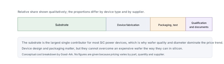
The reason a silicon carbide device costs several times what an electrically comparable silicon part costs is not difficult to understand, and it is almost entirely upstream of the device. The expensive part is the wafer, and the wafer is expensive because growing this crystal is slow, hot and difficult.
Last updated:
The sticker price, honestly
Two effects combine. First, a silicon carbide wafer costs more than a silicon wafer of the same diameter. Second, the industry works with smaller diameters: 150 mm is a common silicon carbide size while silicon power devices are made on 200 mm and logic on 300 mm. A smaller wafer with a higher cost per unit area means fewer devices and a higher cost per device before any processing begins.
For most silicon carbide power devices, the substrate accounts for a large share of the finished device cost. That single sentence explains the shape of the industry: the companies who can grow good crystals cheaply have an advantage that no amount of clever device design can fully compensate for, and the price of the finished part tracks the price of the wafer more than it tracks the complexity of the device.
Why growing the crystal is hard
Silicon can be melted and pulled into a large single crystal by a method that has been refined for seventy years. Silicon carbide does not melt usefully; it sublimes, passing directly from solid to vapour at temperatures above 2000 °C. Crystals are therefore grown by a vapour transport process in which material moves from a source powder to a seed crystal, and the growth rate is measured in millimetres per hour.
Three consequences follow. The process is slow, so each furnace produces less material per day. The temperature is extreme, so equipment wears and maintenance windows are short. And the resulting crystal contains defects — micropipes, dislocations and stacking faults — that are more varied and more consequential than the equivalent defects in silicon. A defect that occupies a fraction of a millimetre can ruin a power device that has to block a kilovolt.
Substrates and yield
Yield is where the economics become uncomfortable. A wafer is only useful in the area where the crystal is good enough, so a higher defect density means a smaller usable area and effectively a higher cost per good device. Defects also propagate: some appear during the growth of the crystal and are inherited by every device cut from that region.
Improving yield is therefore the main lever on price, and it improves with process learning rather than with a single invention. This is why prices have fallen steadily while remaining well above silicon: each year brings better crystal quality and larger wafers, and each improvement removes a slice of the cost rather than the whole gap.
Packaging and testing costs
Packaging costs more for silicon carbide as well, for reasons that follow from the application. Devices operate at high voltage and carry high current, so the internal connection has to be robust: instead of fine wires, many designs use clips or ribbons. The package has to remove heat efficiently, which means better materials and often a larger or more carefully engineered thermal path. And because the switching edges are fast, the package’s internal inductance becomes a parameter rather than a detail.
Testing adds a further cost because the parameters that matter are more numerous. On-resistance has to be checked at temperature, gate behaviour has to be characterised, and the high-voltage screening that protects a supplier’s reputation is not free. None of these is unique to silicon carbide, but the combination of high voltage, high current and fast switching makes each of them more demanding than the silicon equivalent.
What system savings can offset it
The argument for paying the premium rests on what the device lets you remove. A more efficient converter can use a smaller heatsink, and in some designs that removes a fan and its noise. Higher switching frequency shrinks the transformer, the inductors and the capacitors. Higher power density means a smaller enclosure, which in a vehicle means less weight and in a data centre means more compute per rack.
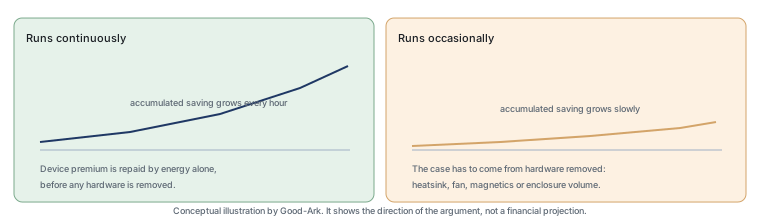
There are also second-order savings that are easy to overlook: fewer cooling parts mean fewer joints and fewer failure modes; smaller magnetics mean less copper; smaller enclosures mean less shipping volume. In equipment that runs for years, the energy saved per hour is the most straightforward of all, because it accumulates without any further engineering effort.
| Cost item | Paid by | Offset by |
|---|---|---|
| Device premium | The bill of materials, at the start | Nothing, until the system is assembled |
| Additional gate drive and layout work | Engineering time | Being designed in once, and re-used across projects |
| Higher-frequency filtering | Extra components and board area | The smaller magnetics the higher frequency allows |
| Thermal design effort | Engineering time | A smaller heatsink and, sometimes, no fan |
| Qualification work | Test time and documentation | Re-use for later products on the same platform |
| Energy lost in operation | Recurring, for the life of the equipment | Every hour of operation, automatically |
Where prices are heading
Three forces point in the same direction. Wafer diameters are increasing, which reduces cost per device area. Crystal quality is improving, which raises yield. And demand from vehicle and energy applications has justified investment in capacity that would not have been built for industrial customers alone. Each of these has already pushed prices down and each has further to run.
The counterweight is that silicon is not standing still either. Silicon power devices keep improving, which means the silicon carbide premium has to be justified against a moving baseline rather than against a part designed ten years ago. That is why silicon carbide has expanded into some market segments and not others: it moves the boundary gradually rather than converting the whole industry at once.
A simple break-even way of thinking
You do not need a model to make a first judgement. Ask four questions in order. What is the efficiency difference between the two options, in percentage points? How many hours a year does the equipment run? What is the value of a kilowatt-hour over the life of the product? And how much hardware — heatsink, fan, magnetics, enclosure — does the more efficient option let you remove?
If the equipment runs continuously, the first three questions usually settle it, because the energy difference compounds over thousands of hours. If the equipment runs occasionally, the answer usually lies in the fourth, and if nothing can be removed, the premium is hard to justify. The point of the exercise is not precision; it is knowing which of the four is doing the work.
If you want to check the material and device claims against an external source, three references are useful. The material is described under silicon carbide, the switching device class under power MOSFETs, and the crystallographic background in our article on crystal growth. Published device measurement methods come from JEDEC, assembly and workmanship expectations from IPC, and sector-level context from the Semiconductor Industry Association. Wide bandgap and sector background is published by IEC, the US Department of Energy and NIST.
Summary
Silicon carbide devices cost more because the crystal is slow and difficult to grow, because wafers are smaller and the substrate dominates the device price, and because packaging and testing are harder at high voltage with fast switching. The premium is repaid by efficiency over time and by the hardware a more efficient converter allows you to remove. That calculation favours equipment that runs continuously and is expensive to cool, which is exactly where the technology has been adopted.
FAQ
Why are silicon wafers so expensive?
Silicon itself is cheap and abundant — it is refined from sand. The cost is in the processing: purification to parts-per-billion cleanliness takes a great deal of energy, crystal growth and slicing require precision equipment, and finishing a large wafer to the flatness and defect levels a modern process demands is difficult. Cost also rises sharply with diameter and with the demands of the most advanced processes. A silicon carbide wafer costs far more again, for the growth reasons described above.
Why is SiC better than silicon?
At high voltage, because it can block the same voltage with a thinner, lower-loss region and waste less energy per switching event. That advantage is conditional rather than universal — at low voltage, silicon is cheaper and entirely adequate. The full comparison is in our article on silicon carbide versus silicon.
What is replacing silicon chips?
Nothing is replacing silicon wholesale, and the phrasing usually oversimplifies a division of labour. Silicon carbide and gallium nitride are taking specific bands: high-voltage power conversion and compact high-frequency supplies respectively. For logic, memory and the overwhelming majority of low-voltage switching, silicon remains dominant and continues to improve. The result is a set of materials used side by side rather than a succession.
Who is the largest manufacturer of silicon carbide?
The question splits in two, because substrates and finished devices are made by different sets of companies, and the leaders differ at each layer. Rankings also move as capacity is added. We have not verified current market-share data for this article, so the honest answer is to point you to published market reports and to manufacturers’ own capacity disclosures rather than to name a leader from memory.
Will SiC prices keep falling?
The structural drivers all point that way: larger wafer diameters, improving crystal quality and yield, and capacity investment justified by vehicle and energy demand. But silicon keeps improving too, so the relevant question is not whether silicon carbide gets cheaper in absolute terms — it is whether the gap narrows relative to the silicon alternative for your application. That gap has been narrowing, which is why the material keeps moving into new segments.
What to do next
Take the four questions in the break-even section and answer them for the product in front of you. If the duty cycle is high, the case is usually straightforward; if it is low, look for hardware you can actually remove, because that is where the justification has to come from. The system-level view of why the material exists is in our guide to Good-Ark SiC devices.
Give Good-Ark the voltage class, the duty cycle and the thermal budget, and we can point to the family that fits and the documentation needed to qualify it.
Email sales@goodark.com, or begin at the SiC portfolio page.
This article is published by Good-Ark, a manufacturer of silicon carbide devices and therefore an interested party in this subject. No prices, market sizes or market-share claims are given; the cost structure is described qualitatively and the break-even logic is presented as a way of thinking rather than a financial model.
Continue through this engineering topic
For the complete selection, design, verification, and troubleshooting path, explore the Silicon Carbide and Wide Bandgap Hub.
Recommended
 Why Does Your Phone Charger Get Warm?Knowledge
 Energy Efficiency Rules Worldwide: How Regulations Shape Component ChoicesKnowledge
 Wide-Bandgap Semiconductors: Adoption Report 2026Knowledge
 The GaN Charger Market: Why Your Next Adapter Is SmallerKnowledge
 Component Lead Times in 2026: What Is Actually Normal NowKnowledge
 China’s Power Semiconductor Industry: Where It Stands in 2026Knowledge