The GaN Charger Market: Why Your Next Adapter Is Smaller
GaN charger market 2026: what gallium nitride changes physically, why adapters shrank, how price and standards shaped adoption, and what to check.
Updated: October 27, 2026
Read GaN charger market dynamics as a planning input for topology and capacity—not as a precise forecast you can enter into an MRP system. Third-party market figures vary by scope; translate them into engineering actions: voltage class mix, package capacity, and lead-time risk.
For device-level follow-ups see power semiconductor market outlook 2026–2030 and silicon carbide market 2026.
| Market signal | Engineering response | Do not |
|---|---|---|
| Demand growth in a segment | Stress-test second sources and MoQ | Scale unique MPNs prematurely |
| Shift to higher V / WBG | Revisit derating and gate-drive | Copy Si designs unchanged |
| Regional capacity headlines | Map real lead times by package | Treat press CAGR as bookings |
| Efficiency regulation pressure | Budget conduction + switching loss | Optimize only sticker VF |
From brick to pocket-sized
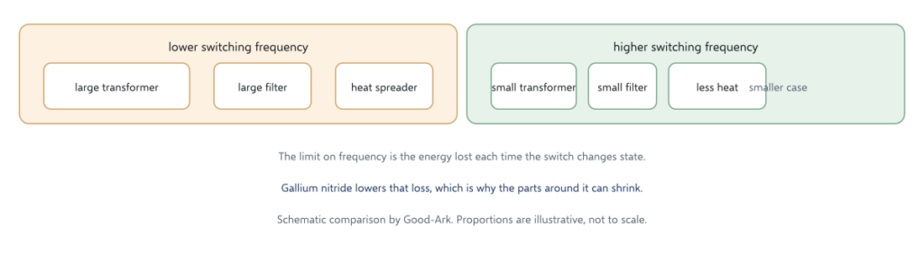
The power adapter that came with a laptop fifteen years ago was a brick with a mains cable, and the size was set by the components needed to handle the power. Two of those components scale with frequency. The magnetic part, which transfers energy across the isolation barrier, and the capacitors that smooth the output, both become smaller when the switching frequency rises, because each switching cycle handles less energy and the smoothing interval becomes shorter.
Silicon switches cannot simply be driven faster, because the energy lost each time they switch rises with frequency, so an attempt to shrink the magnetics by switching faster produces a hotter converter rather than a smaller one. The comparison that fits is a door that has to be opened and closed: doing it more often is only useful if each movement is cheap. Gallium nitride devices make each movement cheaper, which is what allows the frequency to rise and the components to shrink.
What GaN changes physically
The difference is a material property. Gallium nitride has a bandgap of roughly 3.4 electronvolts against silicon’s 1.1, which means a device of the same voltage rating can be built in a much thinner layer with lower resistance. It also has a higher electron mobility in the channel of the transistor that is normally used, so for a given die area the device can carry more current and switch faster.
In a charger that translates into three visible effects. The converter runs at a higher frequency, so the transformer and the filter shrink. The losses per switching event are lower, so less heat has to be removed, which reduces the heat spreader. And the whole power stage can occupy less board area, which allows the enclosure to shrink around it. None of that changes the amount of power delivered; it changes how much space and heat it takes to deliver it.
| Property | Effect in a charger | What it does not change |
|---|---|---|
| Higher switching frequency | Smaller transformer, smaller filter | How much power the output can deliver |
| Lower switching loss | Less heat, smaller heat path | The heat generated by the load itself |
| Higher breakdown field | Thinner device, lower resistance | The isolation and safety requirements |
| Fast switching edges | Design attention to layout and noise | Anything the customer sees |
How the market grew
Three things had to be true at the same time for this category to become ordinary. The devices had to be manufacturable at a cost a consumer product could absorb. A standard had to exist that let a small connector carry enough power to charge a laptop. And the rest of the design had to be able to follow the faster switching without becoming unreliable, which meant better controllers, better layout practice and better magnetics.
The order matters. Standards came before volume, because a charger can only be small if the cable and connector allow the power to pass. Device cost fell as production volumes rose, which happened after the standard made a mass market possible. And the design practice accumulated as engineers learned to control the faster edges that come with the material.
Price parity with silicon
The premium has narrowed for the same reason it narrowed in silicon carbide: yield improves, volumes rise and the process becomes routine. What has not changed is that the gallium nitride device is still more expensive per unit than the silicon switch it replaces, and the charger is cheaper because the components around it are smaller rather than because the switch itself is cheap.
That has a practical consequence for anyone comparing two adapters that look identical. The savings from the smaller magnetics and the smaller enclosure are what pay for the more expensive switch, and a design that takes the expensive switch without taking the size benefit has paid the premium for nothing. It is one reason a nominally similar adapter can be heavier, or run hotter, than another with the same rating.
Where SiC still wins
The two wide bandgap materials are not interchangeable, and the boundary is roughly set by voltage and current rather than by fashion. Gallium nitride devices are strong at the voltages and frequencies a charger works at, which is why the consumer power adapter is their natural home. Silicon carbide devices are strong where the blocking voltage and the current are much higher, such as traction inverters and high-power solar conversion, where the operating frequency is lower and the thermal load is much larger.
The comparison is a sports car and a truck. Both are more capable than a family saloon, and only one of them is useful for moving a load up a hill. For an adapter, gallium nitride; for a traction inverter, silicon carbide; and for an ordinary rectifier at mains voltage, plain silicon, which is still the right answer for most of the parts in the product.
Standards and USB power delivery as a driver
The reason a small adapter can charge a laptop is the standard that governs the negotiation between the charger and the device. The USB Power Delivery specification defines a set of voltage levels beginning at 5 V and rising through 9 V, 15 V and 20 V, with a maximum power of 100 W in the original specification and a later extended range that raises that ceiling to 240 W. The charger and the device negotiate which level to use, so the same port can serve a phone and a laptop.
That negotiation is what makes a universal adapter possible, and it is also why the physical size fell. Before it, a laptop needed a barrel connector and a fixed voltage, which meant the adapter could not be shared. The standard turned the adapter into a commodity with a defined interface, which in turn justified investment in making it smaller.
What to look for when buying
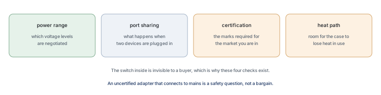
Four things matter more than the material claim. The negotiated power range, because an adapter that supports higher voltage levels can charge more devices faster. The number of ports and whether power is shared between them, because a two-port adapter divides its output when both are in use. The certification marks for the market you are in, because those are the evidence that the safety and efficiency requirements were met. And the physical arrangement, because a compact charger concentrates its heat in a small volume and needs airflow around it.
A safety note belongs here, because the category’s popularity has produced a market in uncertified copies. An adapter that connects to mains voltage is a safety-relevant product, and an uncertified unit may lack the insulation, the creepage distance and the protection that the standards require. The absence of a recognised certification mark is not a stylistic detail.
Outlook
The direction is that the technology keeps moving into smaller and cheaper products as the device cost falls, and the constraint is that the safety and efficiency requirements do not change with the material. Where the next step lies is not in shrinking the adapter further, because the mains interface and the isolation barrier set a floor, but in integrating more of the system into the same package and in using the higher power range the standard now allows.
How to use this report without over-fitting
- Separate what is measured (shipments, ASP bands) from what is opinion (CAGR to 2030).
- Map claims to your BOM families: Si Schottky, FRD, MOSFET, IGBT, SiC.
- Prefer dual-source packages over single-source exotic outlines when volumes are uncertain.
FAQ
Are the market size numbers in articles exact?
Treat them as directional unless you have the primary analyst table and identical scope. Definitions of “power semiconductor” differ widely.
What should purchasing do with a bullish forecast?
Negotiate forecast flexibility, not only price. Ask for package-level lead times and PCN policy.
Does AI / EV demand change discrete diode selection?
It raises current density and thermal expectations in adjacent rails (48 V, AUX, sensors). The diode still needs a normal V/I/thermal worksheet.
Where should engineers go next?
Pair this overview with a concrete selection guide such as power MOSFET selection or power rectifier selection.
Continue through this engineering topic
- Power Semiconductor Market Outlook 2026 2030
- Silicon Carbide Market 2026
- Ai Data Centers Power Semiconductor Demand
- Automotive Semiconductor Report 2026
- China Power Semiconductor Industry 2026
- Component Lead Times 2026
- Power Supply Application Design Hub
Topic hub: Power semiconductor market outlook 2026–2030 — related selection guides and application notes in this cluster.