The Silicon Carbide Market in 2026: Capacity, Prices and Adoption
Silicon carbide market 2026: the three layers of the SiC supply chain, why capacity timing matters, and why prices moved the way they did over the decade.
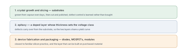
Silicon carbide is the material behind the power devices that made high-voltage switching efficient, and the market around it is best understood as three separate businesses stacked on top of each other: growing the crystal and cutting it into substrates, growing an epitaxial layer on top, and fabricating devices on that. Each layer has its own capacity, its own yield curve and its own timing, and most of the confusion about SiC supply comes from treating the three as one.
Last updated:
Scope and method
This report describes the structure of the silicon carbide supply chain and the reasons capacity and price behave as they do. It does not publish a market value, a price level or a capacity figure, because the sources that do publish such figures use different boundaries — some count substrates, some count devices, some count the whole power market with SiC inside it — and a reader cannot compare them without the definitions attached.
What is used instead are technical constants, which are checkable in any semiconductor textbook. Silicon has a bandgap of roughly 1.1 eV; silicon carbide’s is around three times larger. Silicon carbide also conducts heat several times better than silicon, which matters more than it sounds, because a device’s practical current limit is often set by how fast heat can leave the die rather than by the die itself.
The three layers of the SiC supply chain
The first layer is the crystal. Silicon carbide does not melt and pour the way silicon does, so the crystal is grown from vapour at high temperature over days, and the resulting boule is then sliced. This is the layer where the industry’s difficulty is concentrated: growth is slow, defects are hard to eliminate, and yield improves through experience rather than through buying a machine.
The second layer is the epitaxial layer, a thin film grown on the substrate with a controlled doping level. The device’s voltage rating is largely set here rather than at the substrate, which is why substrate and epitaxy are sold as different products with different specifications, and why a defect that appears in one becomes a device failure in the other.
The third layer is fabrication, where the transistor or diode is built and packaged. At this layer the process is closer to the familiar silicon world, which is why several companies can and do fabricate SiC devices on purchased substrates instead of making their own. That division is the reason a buyer may deal with three different suppliers for what looks like one product line.
| Layer | What it produces | Where the difficulty sits |
|---|---|---|
| Crystal growth and slicing | Substrates in wafer form | Slow growth, defect control, yield |
| Epitaxy | A doped layer whose thickness sets the voltage class | Uniformity and defect carry-over from the substrate |
| Device fabrication and packaging | Schottky diodes, MOSFETs, modules | Process control, gate reliability, thermal packaging |
Capacity additions and timing
Capacity in this chain is added in lumps and arrives years after the decision to build. A substrate furnace line, an epi reactor and a device fab each have their own lead time, and they have to be balanced against each other: adding device capacity without adding substrate capacity simply moves the queue. That imbalance explains the pattern where device makers announce expansions that cannot be fully used until the material layer catches up.
The comparison to a bakery is close enough to be useful. Ovens cannot be added overnight, and adding ovens is pointless if the flour mill has not expanded. In the same way, the visible announcement is often the last step of a chain whose constraint is somewhere upstream, and the practical question for a buyer is which layer the promised capacity belongs to.
Price movement and why it stalled adoption
Silicon carbide devices entered the market at a substantial premium to silicon, and that premium is the reason adoption has followed the applications where efficiency is worth paying for: traction inverters in electric vehicles, high-power solar conversion, and the highest-density power supplies. Where the efficiency gain does not pay back the price difference, silicon has continued to be the rational choice, and pretending otherwise misreads the market.
Two mechanisms have been reducing the gap. The first is yield: as crystals are grown with fewer defects and more of each wafer becomes usable, the cost per good device falls without any change in the process. The second is scale, because a wider wafer yields more devices per growth run for the same time in the furnace. Neither mechanism is fast, and neither follows a schedule that can be promised to a buyer a year ahead.
A separate confusion is worth clearing up, because it appears in search results. There is an industrial material sold by weight and called silicon carbide that is used as an abrasive and as a refractory, and there is electronic-grade silicon carbide sold as wafers with a defect specification. They are different products with different purity requirements and different markets, so a price per tonne for the abrasive says almost nothing about the cost of a device wafer.
Demand from EVs and PV
The two demand centres that matter most are traction electronics and power conversion. In an electric vehicle the benefit is not only efficiency but packaging: a device that wastes less heat needs a smaller cooling system, and in a vehicle the cooling system has weight, volume and cost of its own. That is why the technology appeared first in vehicles designed around a high-voltage battery rather than in the smallest consumer products.
In solar and storage the same argument appears in a different form. Conversion efficiency is measured over the life of the installation rather than over a drive cycle, which favours a device whose losses are lower every hour of every day. The counterweight is capital cost, which is why the migration in that sector has been gradual and why silicon insulated-gate bipolar transistors remain in a great deal of installed equipment.
Who makes what, regionally
Rather than a ranking, it is more useful to know the shapes of the businesses. Some companies make substrates and sell them, some buy substrates and sell devices, and some do both, which means a single supplier relationship can cover one layer, two or all three and buyers often cannot tell which from a catalogue entry. The substrate layer is the most concentrated, because crystal growth knowledge accumulates slowly. Device fabrication is more widely spread, because it can be built on purchased material.
What could change the forecast
Four things would move the picture materially. A step change in substrate yield would lower device cost without any new capacity. A design change that reduces the amount of material used per device would have a similar effect. A slowdown in the two main demand centres would leave the new capacity idle and soften prices. And a competing technology improving enough to close the efficiency gap at a lower cost would change which applications adopt which material.
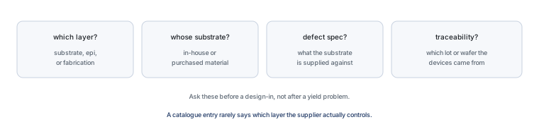
Each of those is a condition with an observable signal rather than a prediction, which is the honest form for this kind of statement. What a buyer can do is watch the layer that constrains the parts they use, and ask a prospective supplier which layer of the chain it controls.
Numbers to watch
The numbers that carry information here are not market totals. They are the defect specification of the substrate a supplier buys, the wafer diameter it works on, the yield it reports internally, the voltage classes it actually ships, and the lead time for a repeat order. Those five describe a supplier’s position in the chain more reliably than any published market figure, and all five can be asked for directly.
FAQ
Is silicon carbide the future of power electronics?
It is the future of the part of power electronics where high voltage and high efficiency justify a higher device cost, and silicon remains the practical choice everywhere that is not true. The honest answer is therefore “in some applications”, and the applications are identifiable: traction conversion, high-power solar and storage, and the densest power supplies.
What is the current price of silicon carbide per ton?
That question belongs to a different industry. Silicon carbide is also made in bulk as an abrasive and refractory material and sold by weight, while electronic-grade material is sold as wafers measured in millimetres of diameter with a defect specification. A commodity price per tonne therefore carries almost no information about the cost of a device wafer.
Why is silicon carbide more expensive than silicon?
Because the crystal is grown from vapour over days rather than pulled from a melt, because defects are harder to eliminate, and because the industry is working at a smaller scale with a shorter learning history. All three are yield and experience problems rather than fundamental ones, which is why the premium has fallen gradually rather than in a single step.
Does a silicon carbide device always save energy?
It has lower switching and conduction losses at the ratings it is designed for, so in a well-matched design it reduces losses. In a design where the device is used far below or far above its intended operating range, the advantage can shrink or disappear, and the extra cost buys nothing. Whether it saves energy is a question about the operating point, not about the material by itself.
What to do next
Ask a prospective supplier which layer of the chain it controls and whose substrate it uses. Those two answers tell you more about supply security than any market figure. The device-level comparison between the two silicon carbide families is in choosing between a SiC diode and a SiC MOSFET, the wider material picture is in what silicon carbide is, and the portfolio view is in the silicon carbide device families.
Background material is available from the Semiconductor Industry Association on the sector, the material itself, device standards from JEDEC, electrotechnical standards from IEC, quality management from ISO, and energy-technology context from the US Department of Energy. Sector and energy background is published by NIST.
Tell Good-Ark the voltage class, the switching frequency and the cooling available, and we will tell you which device family fits and what the ordering unit is.
Email sales@goodark.com, or start from the silicon carbide portfolio.
This article is published by Good-Ark, a manufacturer of discrete semiconductor devices. It is a structural report and publishes no market value, price level or capacity figure; the material constants quoted are textbook values, not measurements of a market.
Continue through this engineering topic
For the complete selection, design, verification, and troubleshooting path, explore the Silicon Carbide and Wide Bandgap Hub.
- Practical guide: Running SiC Hot: Junction Temperature, Power Cycling, and Reliability Evidence
- Practical guide: SiC Schottky Barrier Diodes: Why the 1700 V SBD Exists and Where It Pays
- Practical guide: SiC SBD or SiC MOSFET: Choosing the Silicon-Carbide Device That Fits the Duty
- Ask Good-Ark technical support about this application
Recommended
 Why Do Diodes Get Hot? Conduction and Switching Losses ExplainedInfoStandard, Fast Recovery, and Schottky Diodes: What’s the Difference?Info
 What Is a Fast Recovery Diode? Understanding “Fast Recovery”Info
 What Is a Diode? A Beginner’s Guide to How It WorksInfo
 Automotive Semiconductor Report 2026: Chips Per Car Keep RisingKnowledge