How Does a Diode Work? The PN Junction in Plain Language
How does a diode work? Two regions of treated silicon, one boundary, and a zone that appears where they meet, which decides everything about the behaviour.
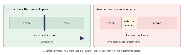
Everything a diode does comes from one thin boundary inside it. The package, the leads and the markings are just delivery; the behaviour lives in a zone a few micrometres wide where two differently treated regions of silicon meet, and understanding that zone makes the rest of the device class predictable rather than mysterious.
Two kinds of silicon, one junction
Pure silicon is a poor conductor. To make it useful, manufacturers introduce small amounts of other elements — a process called doping — which changes how many free charge carriers the material has. Doping with an element that donates extra electrons produces what is called n-type material, where the majority carriers are negative. Doping with an element that leaves a deficit produces p-type material, where the majority carriers behave as positive.
Neither type is remarkable on its own. What makes a diode is putting them together. Where the two regions meet, carriers diffuse across the boundary and recombine, leaving behind a zone with almost no free carriers at all. That zone is the depletion region, and it is the part of the device that does the work.
What happens when you push electrons
Connect a supply so that the p-type side is positive relative to the n-type side and the depletion region collapses. The zone with no carriers shrinks to almost nothing, current flows freely, and the diode is in forward conduction. Reverse the supply and the opposite happens: the region widens, current is blocked, and only a tiny leakage current flows.
The analogy that gets this across without a physics lecture is a hill in a pipe. Forward bias lowers the hill until water flows over it; reverse bias raises the hill until nothing gets through. The useful part of the picture is that the hill is not a flap that opens and closes — it is a region whose height depends on the voltage across it, which is why a diode responds continuously rather than snapping between states.
Why 0.7 volts appears
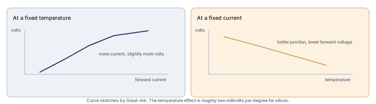
Before forward current can flow freely, the applied voltage has to overcome the barrier that the depletion region presents. For a silicon junction, that crossover happens at around 0.6 to 0.7 volts, which is why the number appears everywhere in datasheets and textbooks. It is not a threshold that switches the device on; it is the point on a curve where the current starts to rise steeply.
Two details make the number less mysterious. It changes with current: push more current through and the voltage rises a little above 0.7. And it falls as temperature rises, by roughly two millivolts per degree Celsius for silicon. That last property is the reason a diode can be used as a crude temperature sensor, and the reason forward voltage measured on a bench rarely matches the single typical figure on a datasheet.
The depletion region, simply
The depletion region is not an empty space. It is a zone where the fixed charges left behind by diffused carriers create an internal electric field. That field is what opposes further diffusion, producing an equilibrium where the tendency of carriers to spread out is balanced by the field pushing them back.
Once you see the region as a balance rather than a gap, several behaviours become obvious. Applying voltage in one direction weakens the field, so the balance tips toward conduction. Applying it the other way strengthens the field, so the region widens and blocks harder. And the region has capacitance, because it is two layers of charge separated by an insulating zone — which is why fast signals care about the diode type they pass through.
What breaks down in reverse
Reverse blocking is not unlimited. Increase the reverse voltage far enough and the internal field becomes strong enough to free carriers directly, and the device starts to conduct in the direction it was supposed to block. In an ordinary rectifier this is destructive. In a Zener or a TVS diode it is deliberately engineered and controlled, which is how those devices clamp a voltage.
The breakdown voltage is therefore a design parameter rather than a failure. The same physical event is a fault in one product family and the entire working principle in another, which is a useful reminder that device classes are defined by intent and specification rather than by a different kind of silicon.
Where the heat comes from
Heat appears wherever energy is converted to heat, and in a diode there are two places. The first is forward conduction: current passes through a region with a voltage across it, and the product of voltage and current is power dissipated in the device. The second is switching: each time the diode changes state, a small amount of energy is lost in the transition, and the amount depends on how fast the carriers can be cleared from the junction.
That second loss explains why diode families exist at all. A junction optimised for low forward voltage tends to be slower to clear, while one optimised for fast recovery tends to have a higher forward voltage. The trade is a consequence of the same physics, and it is the reason no single diode is best in every circuit.
| Property | Ordinary silicon rectifier | Schottky rectifier | Fast recovery rectifier |
|---|---|---|---|
| Forward voltage | Around 0.7 V, rising with current | Lower, often a few tenths of a volt | Higher than a Schottky, similar to or above an ordinary rectifier |
| Reverse recovery | Slow, because stored carriers must clear | Very fast, because there is little stored charge | Fast by construction |
| Usable voltage range | Wide, up to high voltages | Limited, which is the key constraint | Wide |
| Leakage when hot | Low | Higher, and it grows quickly with temperature | Low |
| Typical use | Mains-frequency rectification | Low-voltage outputs in switching supplies | High-frequency rectification at higher voltage |
Why this matters for real circuits
Three practical consequences follow from the junction. First, forward voltage becomes heat, so a diode carrying a lot of current in a small package needs a thermal path. Second, reverse recovery matters whenever the current changes direction quickly, so high-frequency circuits choose diode families accordingly. Third, leakage grows with temperature, which can become self-reinforcing in a Schottky device: heat raises leakage, leakage raises heat. That mechanism is covered in our article on Schottky thermal runaway.
None of those three is visible from the symbol on a schematic. They are all consequences of the physics inside, which is why the same symbol can represent a part carrying two amps with no heatsink and a part carrying two hundred amps bolted to an aluminium plate.
It is worth separating two questions that beginners tend to merge. One is how the device behaves, which is physics, and the other is whether a particular part is suitable for a particular position, which is specification. The physics is fixed and shared by every diode of a given family; the specification is per part and per operating condition. A surprising share of beginner frustration comes from answering the first question carefully and then treating the second as if it followed automatically.
Common beginner questions
The question that comes up most often is whether this level of detail is necessary. The honest answer is that you can build and repair circuits without it, and you will make fewer mistakes with it. Knowing that forward voltage falls as temperature rises explains why a diode that measured well on the bench can misbehave inside a hot enclosure. Knowing that leakage grows quickly with heat explains why a Schottky output stage can fail on a warm day. And knowing that reverse breakdown is a designed property in some families explains why a Zener does not simply “leak”.
The related reading on this site covers the PN junction, diodes and the band gap. Device measurement methods come from JEDEC, board assembly expectations from IPC, and sector-level material from the Semiconductor Industry Association. Device and assembly background is published by ISO, NIST and IEC.
FAQ
What kills diodes?
In rough order of frequency: too much forward current, which overheats the junction; a reverse voltage beyond the rating; a surge exceeding the device’s non-repetitive capability; and thermal fatigue from repeated heating and cooling. Manufacturing defects exist but are a small share of real failures. The process side of this — how a junction is built and where quality can be lost — is covered in our article on how diodes are manufactured.
How does a diode stop current flow?
By widening the depletion region rather than by closing a physical contact. When the applied voltage reverses, the internal field in that region grows, the zone with almost no free carriers becomes wider, and the barrier that carriers would have to cross becomes too high for them. It is not a perfect stop: a small leakage current continues, and it grows with temperature.
Does a diode work on AC or DC?
It works on either, and the choice of circuit decides the meaning. Feed a diode alternating current and it will conduct on one half of the cycle and block the other, which is the basis of rectification. Feed it direct current in the forward direction and it conducts; feed it direct current in reverse and it blocks. The device responds to the voltage across it at each moment rather than to any label on the supply.
Are diodes still used today?
In larger volumes than ever. Almost everything that plugs into a wall socket rectifies at some point, every battery-powered device protects against reverse connection, and solar modules carry bypass diodes to survive shade. The fact that a component is simple and old says nothing about its volume; rectifier diodes are among the highest-volume electronic parts manufactured.
Why does the forward voltage change between two diodes of the same type?
Because it depends on current density, junction temperature and process variation, and a datasheet can only quote a typical value with conditions attached. Two parts from the same reel will be close, and two measurements taken at different currents or temperatures will not. When comparing parts, compare them at the same conditions or the comparison is meaningless.
What to do next
If you have a diode and a meter, run the two experiments in the figures above: measure forward voltage at two different temperatures, and note how the reading moves. That single observation turns the junction from an abstraction into something you have seen. The practical consequences for heat are covered next in our article on why diodes get hot.
Tell Good-Ark the voltage, the current and the switching frequency, and we can point to the family that fits and explain the trade-offs the choice commits you to.
Email sales@goodark.com, or start from the product family learning centre.
This article is published by Good-Ark, a manufacturer of diodes and other discrete devices. Junction behaviour is described at a level intended for beginners; exact values depend on the part and its operating conditions and belong to the official datasheet.
Continue reading
Browse the Rectifier Selection and Ratings for related guides.
Recommended
 Why Do Diodes Get Hot? Conduction and Switching Losses ExplainedInfoStandard, Fast Recovery, and Schottky Diodes: What’s the Difference?Info
 What Is a Fast Recovery Diode? Understanding “Fast Recovery”Info
 What Is a Diode? A Beginner’s Guide to How It WorksInfo
 Automotive Semiconductor Report 2026: Chips Per Car Keep RisingKnowledge