Si MOSFET Power Switching for SMPS, PV Inverters, and Automotive Designs
Updated: October 28, 2026 Silicon MOSFETs remain the default power switch in many SMPS stages, mid-power PV inverter legs, and automotive DC…
Updated: October 28, 2026
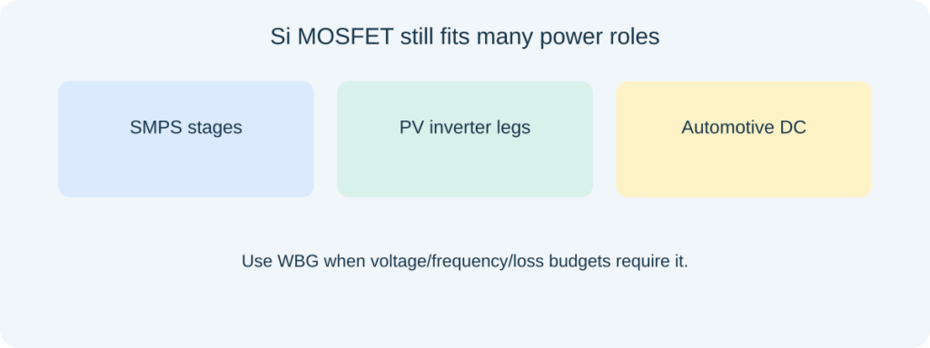
Silicon MOSFETs remain the default power switch in many SMPS stages, mid-power PV inverter legs, and automotive DC rails where voltage, cost, and ecosystem maturity still favor Si. Wide-bandgap devices earn their place when loss, frequency, or voltage targets demand them—but a reliable Si MOSFET choice still starts with ratings, drive, thermal path, and body-diode behavior matched to the topology.
When a Si MOSFET is still the right switch
Choose silicon when the bus voltage, switching frequency, and loss budget fit Si technology and the drive ecosystem is already proven.
Catalog hubs from ST and application notes such as Infineon’s Power MOSFET Basics document the same core parameters buyers and designers argue about: breakdown voltage, RDS(on), threshold, gate charge, and diode forward behavior. PCIM explainers on MOSFET-as-switch behavior help newcomers; production designs need those parameters under hot, biased conditions.
For high-voltage rating detail on this site, continue with the high-voltage MOSFET design checks article. This page focuses on application-oriented Si selection across SMPS, PV inverter, and automotive power paths.

Datasheet checks that decide reliability
| Parameter | Why it matters | Compare at |
|---|---|---|
| VDSS / V(BR)DSS | Must cover bus peaks and ringing with margin | Worst-case clamp waveform |
| RDS(on) | Conduction loss and hot rise | Hot Tj and actual VGS |
| Qg, Qgd | Driver stress and switching loss | Same VGS swing as the driver |
| Body diode VF / trr | Hard-switched bridges and sync paths | Expected diode conduction events |
| Thermal Rth | Package alone does not cool the die | Installed copper or heatsink |
Infineon’s basics article stresses that on-resistance and gate charge trade with die size and voltage class. A “lower RDS(on)” alternate that doubles gate charge can overheat the driver or slow transitions enough to erase the conduction win.
SMPS: primary and secondary switch roles
In flyback, forward, and half-bridge SMPS stages, the Si MOSFET sees a combination of magnetizing or reflected currents and leakage-induced spikes. Clamp networks must keep voltage inside the MOSFET rating with margin. Synchronous secondary MOSFETs add body-diode conduction during dead time—check diode behavior and dead-time settings together.
Efficiency articles for switch-mode converters show how switching and conduction losses share the budget. Validate both at the minimum input voltage (often highest primary current) and at high line (often highest voltage stress). See also the site’s SMPS overview for stage context.
PV inverters: where Si still appears
String and hybrid inverter architectures increasingly use SiC or other WBG devices in high-voltage stages, yet silicon MOSFETs and IGBTs still appear in auxiliary converters, lower-voltage buses, and cost-optimized legs. The decision is stage-specific. Public PV and inverter explainers on this blog—such as how semiconductor devices enable PV inverters—outline the system roles without claiming one die technology owns every switch position.
For any Si MOSFET in a PV path, confirm humidity/pollution creepage for the package, repetitive avalanche expectations if the design allows it, and gate-oxide stress under long outdoor life. Do not transfer a SiC gate-drive recipe unchanged onto a Si part.
Automotive power rails and switching
Automotive 12 V / 48 V and higher traction-adjacent rails impose ISO/OEM transient sets defined by the program. Si MOSFETs are widely used for DC-DC, motor drives, and load switches when ratings and qualification files match. Request the exact evidence package (AEC references, PPAP level, or OEM list) that your program already uses—do not infer qualification from a catalog adjective.
PCIM-style tutorials show enhancement-mode MOSFETs as switches with clear on/off regions. Vehicle designs add continuous short-circuit and thermal-protection strategies that must be compatible with the MOSFET’s SOA curves.

Si versus WBG: a practical boundary
Move toward SiC or GaN when the combination of bus voltage, frequency, and thermal limits makes Si loss or magnetics size unacceptable—and when the gate-drive and EMI plan are ready. Stay with Si when those constraints are met and supply chain depth matters. Hybrid designs that mix technologies by stage are normal; they are not a failure to “standardize.”
Toshiba and other vendors publish electrical-characteristic application notes that walk through capacitance and switching figures of merit. Use them to interpret datasheets, not to invent a universal winner.
Gate drive and layout minimums
Kelvin source connections for power packages, short gate loops, and adequate decoupling at the driver supply reduce the chance that a correctly rated Si MOSFET still fails from induced turn-on or uncontrolled ringing. If you change package (for example DPAK to TOLL), revisit both thermal and inductance—not only RDS(on).
Good-Ark context
Good-Ark’s public product scope emphasizes discrete diodes, rectifiers, bridges, and related lines; MOSFET coverage on third-party discussions should be verified against current product listings and datasheets before any sourcing claim. Application pages mention SMPS, PV inverter, and automotive lighting/EPS-type contexts at company level. Keep device claims limited to documented parts.
Frequently asked questions
Does a lower RDS(on) always run cooler?
No. Switching loss, drive strength, and thermal interface can dominate. Compare total loss at the operating point.
Can I drop a SiC MOSFET into a Si footprint?
Not without reviewing gate-drive voltage, protection, and EMI. Package similarity is not electrical equivalence.
What is the first waveform to capture on a new Si MOSFET?
Drain-source voltage for overshoot against VDSS, plus gate waveform for clean turn-on/off without excessive ringing.
Why keep “july-2026” in this URL?
The slug preserves the historical address for search continuity. The technical guidance is date-stamped via the update note, not the month in the path.
Continue through this engineering topic
- High-voltage MOSFET design checks
- What is a switching power supply?
- PV inverters and semiconductor devices
- IGBT guide for power switching
Topic hub: High-voltage MOSFET design checks — related power-switch guides in this cluster.
Recommended
 Gate, Drain, Source: The Three Pins of a MOSFET Explained With a Water AnalogyKnowledge
 The Silicon Carbide Market in 2026: Capacity, Prices and AdoptionKnowledge
 What Is a TVS Diode? Surge Protection Explained SimplyKnowledge
 What Static Electricity Really Does to Your ElectronicsKnowledge
 Zener Diodes: Voltage Regulation, Circuit Protection, and ProcurementKnowledge
 Automotive Bridge Rectifier Module: A Practical B2B Buying GuideKnowledge