What Static Electricity Really Does to Your Electronics
Static electricity and electronics: the shock you feel is the visible part. How discharge damages semiconductors, and why it shows up months later.
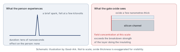
You feel a spark when it reaches a few thousand volts, but a semiconductor can be destroyed by a discharge you never notice — and often is. The interesting part of static damage is not the spark; it is the fact that a device can pass a functional test after the event and fail in the field months later.
Last updated:
How much voltage is in a doorknob shock
The human body charges like a small capacitor, and the discharge when you touch something conductive delivers that charge in nanoseconds. The commonly quoted figures in the ESD industry put the threshold of feeling at roughly two to three kilovolts, with walking across a synthetic carpet in dry air able to build tens of kilovolts. The current is small in absolute terms and extremely brief, which is why the event does not usually hurt you.
What matters for electronics is not the total energy but the concentration of it. A few kilovolts delivered into a structure that is micrometres across is an enormous electric field at that scale. The same event that makes your fingertip tingle can exceed the breakdown strength of the thin oxide layer that forms the gate of a modern transistor.
What happens inside a chip
Three mechanisms account for most static damage. The first is oxide breakdown: the insulating layer under a transistor gate is a few nanometres thick, and a discharge can puncture it, creating a permanent conductive path where there should be an insulator. The second is junction damage, where the current density in a small area melts or migrates the silicon and changes the device’s electrical behaviour. The third is conductor damage, where a thin metal track or bond wire carries more current than its cross-section allows and opens or partially melts.
The first mechanism is the one that makes modern devices more rather than less sensitive. As transistors have shrunk, the gate oxide has thinned faster than the voltages used to program or drive them have fallen, so the margin between normal operation and breakdown is smaller than it was thirty years ago. Devices became more capable and, at the pin level, less forgiving.
Damage you can see versus damage you cannot
Catastrophic damage is the easy case: a pin shorted, a device that fails a functional test immediately, sometimes a visible crater under magnification. It is inconvenient and honest. The harder case is latent damage, where the discharge weakens an oxide or a junction without breaking it, and the device continues to work — passings every test on the line.
Latent damage then surfaces as a shorter service life. The weakened structure is more susceptible to the next stress: thermal cycling, an inrush event, a normal operating voltage that the undamaged device would have tolerated indefinitely. This is why a field failure rate that looks inexplicably high sometimes traces back to handling rather than to the design, and why assembly-line ESD control is treated as a process discipline rather than a courtesy.
Which devices are most at risk
Sensitivity is roughly a function of how small the sensitive structure is and how thin the insulating layer is. Devices with thin gate oxides — microcontrollers, memory, analog parts with small geometry — are at the top of the list. So are devices with exposed high-impedance inputs, laser diodes, RF parts, and anything whose pins connect directly to a structure without a protection network built in.
At the other end, a power rectifier in a large package is comparatively robust, because its sensitive area is large and its junctions are deep. This creates a useful rule of thumb for beginners: the small parts are the fragile ones, and the parts you handle most casually are often the ones that can take the least abuse.
Five habits that prevent damage
The professional approach is a combination of controlling charge generation, controlling discharge paths and verifying that both are working. Five habits capture most of the benefit for someone working at a bench.
- Equalise potentials before touching. Touch a grounded surface, or work on a dissipative mat connected to ground, so that you and the board reach the same potential rather than discharging into each other.
- Keep parts in their packaging until use. A device sitting loose on a bench is accumulating charge through its pins.
- Handle boards by the edges. Fingers on a connector or a component body are fingers on a conductive path.
- Reduce charge generation. Avoid sliding boards across synthetic surfaces, and keep the workspace free of loose plastic film and foam that generates charge easily.
- Raise humidity, or compensate for it. Dry air holds charge longer. In a heated room in winter, the same handling that is safe in summer becomes risky, which is why many labs humidify or use ionisers.
What anti-static bags really do
Not all pink bags are the same, and the differences matter if you are storing parts for a long time.
| Type | How it works | Good for | Limit |
|---|---|---|---|
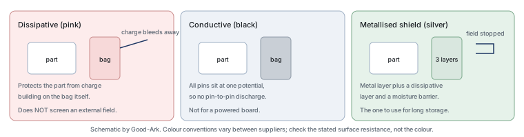
| Dissipative (often pink) | Slowly bleeds charge away rather than insulating it | Protecting parts from charge accumulating on the bag itself | Does not shield against an external field |
| Conductive (often black) | Provides a low-resistance path so all pins sit at one potential | Short-term protection of pins during transport | Must not contact a powered board; can be a short-circuit risk |
| Metallised shield (often silver, translucent) | Combines a metal layer, a dissipative layer and a moisture barrier | Storing or shipping sensitive parts for long periods | Costs more; loses effectiveness if the metal layer is creased through |
The practical conclusion is that a pink bag protects the part from the bag, while a metallised shield bag protects the part from the world. For a hobbyist storing a handful of microcontrollers, either is far better than a plastic drawer. For a production line storing reels for months, the shield bag and humidity control are the ones doing the work.
When the damage shows up months later
Latent damage is not detectable with a multimeter, and it is not detectable with a functional test, which is exactly why it is expensive. The affected device passes on the line and fails in the field, and the failure is attributed to the design or to the component supplier rather than to handling, because by then the evidence has gone.
This is the reason assembly lines measure and audit ESD control rather than relying on operator care. A grounded bench, a logged wrist strap test and an ioniser are cheap compared to a field failure rate that nobody can explain. The same logic applies at a smaller scale to anyone who repairs electronics: the habits are cheap, and the failure they prevent is invisible until it is expensive.
If you want to read further, four external sources are useful starting points: the general explanation of electrostatic discharge, the measurement and standards material published by the US National Institute of Standards and Technology, the test waveforms behind the industry figures from the International Electrotechnical Commission, and the device-level test methods at JEDEC. On the manufacturing side, IPC covers assembly expectations and the Semiconductor Industry Association publishes sector-level material. Standards and measurement background is published by ISO.
Myths worth dropping
Four beliefs cause most of the avoidable damage. “If it still works, it is fine” ignores latent damage. “Static only matters in winter” inverts the mechanism: winter matters because indoor air is dry, so the effect depends on humidity rather than on the season. “Modern chips have protection, so it does not matter” confuses a designed-in network with immunity — every protection structure has a limit and a response time. And “I touched the case first, so I am grounded” only holds if the case is actually connected to earth, which for most bench equipment and most laptops it is not.
FAQ
Can static electricity harm electronics?
Yes, and in three ways: catastrophic failure that shows immediately, latent damage that shortens life without failing a test, and upset conditions where a device resets or misbehaves without permanent damage. The second is the most expensive because it is invisible at the point of occurrence. Devices with thin gate oxides and small geometry are the most sensitive.
How to ground yourself before touching electronics?
Touch a known grounded metal surface first and keep working on a dissipative mat that is connected to the same ground. If you use a wrist strap, use a proper one with a built-in resistor; it is designed to bleed charge slowly, not to carry current. Disconnect power before any of this, because a wrist strap and a live circuit are a dangerous combination rather than a protective one.
What causes a person to have so much static electricity?
Charge builds when two dissimilar materials touch and separate, which is why walking on carpet, sliding off a car seat or unrolling plastic film all charge a person. Dry air keeps the charge from draining away, so the same activity produces a higher voltage in a heated room than in a humid one. Footwear and clothing materials change the amount substantially.
How to get rid of static electricity on electronics?
Do not try to “discharge” a board with a tool or a finger. Instead, equalise potentials: connect yourself to ground through a dissipative path before touching anything, and let the charge equalise over a moment rather than in a spark. For stored parts, move them only inside their packaging, and open that packaging inside the same controlled area where you will handle them.
Do ESD protection diodes make handling safe?
They reduce risk; they do not remove it. On-board protection is designed for a specified event at a specified pin, and it has limits on energy and on response time. Handling damage can occur at a pin the protection does not cover, or at an energy above the part’s rating. Protection and handling discipline solve different halves of the same problem, which is why both exist.
What to do next
Set up one controlled spot at your bench: a dissipative mat, a proper wrist strap with a resistor, and a habit of touching ground before picking anything up. That is a small investment against a failure mode that is otherwise invisible until it costs a product recall. The design side of the same subject is covered in the article on board-level ESD protection, and the general component background in the product family learning centre.
Good-Ark can point to the protection families used at connectors and high-speed interfaces, and explain which part classes suit which line.
Contact sales@goodark.com, or start with the ESD protection diode example.
This article is published by Good-Ark, a manufacturer of protection devices. Discharge voltage ranges quoted here are the commonly published ESD-industry figures used for orientation, not measurements performed for this article.
Continue through this engineering topic
For the complete selection, design, verification, and troubleshooting path, explore the TVS ESD and Surge Protection Hub.
- Practical guide: Zener vs Avalanche vs TVS for Spikes: The Clamping Family Nobody Names Correctly
- Practical guide: Low-Capacitance ESD Diodes: Protecting Signal Pins Without Blurring the Eye Diagram
- Practical guide: TVS, MOV, Zener, or Plain Diode: Which Clamps Your 12 V Rail Safely
- Ask Good-Ark technical support about this application
Recommended
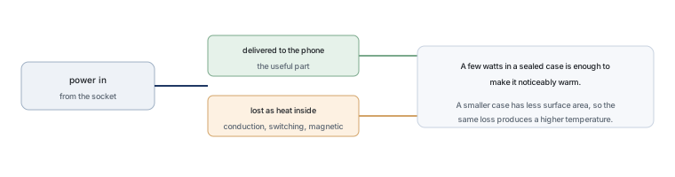 Why Does Your Phone Charger Get Warm?Knowledge
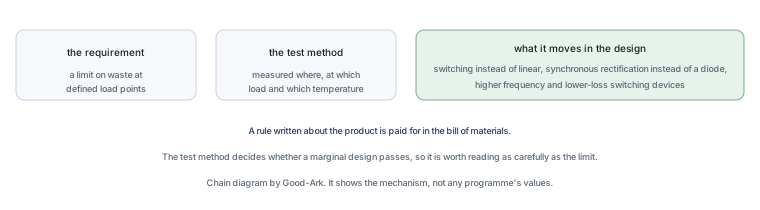 Energy Efficiency Rules Worldwide: How Regulations Shape Component ChoicesKnowledge
 Wide-Bandgap Semiconductors: Adoption Report 2026Knowledge
 The GaN Charger Market: Why Your Next Adapter Is SmallerKnowledge
 Component Lead Times in 2026: What Is Actually Normal NowKnowledge
 China’s Power Semiconductor Industry: Where It Stands in 2026Knowledge