What Is Silicon Carbide (SiC)? A Beginner’s Introduction
What is silicon carbide? The material in sandpaper and in a fast charger share a name. What it is, why its structure matters, and why power devices use it.
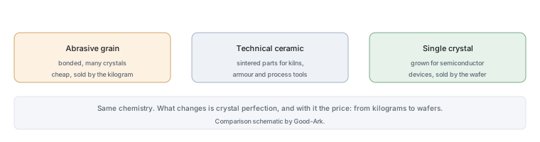
There is a reasonable chance you have held silicon carbide in your hand without knowing it, because the same material that makes an abrasive disc also makes a power transistor. The difference between the two is not chemistry but crystal quality: a bonded mass of hard grains and a single crystal grown for electronics are the same substance at very different levels of perfection.
Last updated:
The material you have probably touched
Silicon carbide is a compound of silicon and carbon, and in bulk form it is one of the hardest materials manufactured at scale — around nine to nine and a half on the Mohs scale, below diamond and roughly comparable to some of the hardest tool materials. That hardness is why it has been used since the late nineteenth century in grinding wheels, abrasive papers and cutting tools, and why it appears in refractory linings and ceramic armour.
A second familiar appearance is jewellery: synthetic silicon carbide is sold as a diamond simulant under the name moissanite, chosen because it is hard, clear and dispersive. A third is inside semiconductor factories, where silicon carbide parts are used in equipment that has to survive high temperatures and corrosive conditions.
Why the crystal structure matters
Silicon carbide is not one material but a family of them. The silicon and carbon atoms can stack in different repeating patterns, and each pattern — called a polytype — has slightly different electrical properties. The two you will meet in datasheets are 4H and 6H, with 4H being the one used for power devices because its properties suit vertical current flow.
That detail matters because it explains why material figures are always approximate. When a text says silicon carbide has a bandgap of about 3.2 electronvolts, it is quoting a value for one polytype; 6H is lower, and the number shifts with temperature as well. Treat material constants as orders of magnitude rather than as specifications, and take device specifications from the device datasheet.
Sand, silicon, silicon carbide
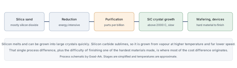
The three are related but distinct, and the relationships are worth untangling because they explain the cost. Sand is mostly silicon dioxide. Reduce it with carbon in a furnace and you get metallurgical-grade silicon, which is refined further for electronics. Combine silicon and carbon directly at high temperature and you get silicon carbide — a compound rather than an element, and one that is much harder to grow as a perfect crystal.
That last point is the root of the price difference. Silicon melts at around 1414 °C and can be grown into large single crystals by well-established methods. Silicon carbide does not melt in a useful way; it sublimes, so crystals are grown by a vapour process at temperatures above 2000 °C, at growth rates measured in millimetres per hour. Slower growth, higher temperature and harder material add up to a more expensive wafer.
What makes it survive higher voltages
The property that matters for power devices is the critical electric field: the field strength at which the material starts to conduct when it should be blocking. For silicon carbide this is roughly an order of magnitude higher than for silicon. A device therefore needs a much thinner region to block the same voltage, and because resistance scales with thickness, the device conducts with proportionally less loss.
The bandgap is the underlying reason. Silicon’s bandgap is about 1.1 electronvolts; 4H silicon carbide’s is about 3.2. A wider gap means more energy is needed to free an electron, which raises the field the material can withstand and also reduces the leakage current at high temperature. That is what the term “wide-bandgap” means in practice, and it explains why the same label covers both silicon carbide and gallium nitride.
Why heat is easier to remove
Here it is worth correcting a common oversimplification. Silicon carbide does conduct heat better than silicon — published values for 4H-SiC are roughly two to three times those of silicon — so heat spreads away from the junction more readily. But the packaged device’s maximum allowed junction temperature is often in the same range as a silicon power device, so the advantage is not that the part can run dramatically hotter.
The real benefit is a combination. Because the device loses less energy in the first place, there is less heat to remove; because the die can be smaller for the same rating, converters shrink; and because the material conducts heat well, what heat there is spreads into the package more effectively. The practical result for a designer is a smaller thermal budget, which is a system advantage rather than a single number on a datasheet.
Other uses beyond electronics
Away from power devices, silicon carbide is used as an abrasive in grinding and cutting, as a refractory material in kilns and furnaces, as a component in ceramic armour, and as a structural material in high-temperature equipment. It also appears inside semiconductor manufacturing itself, in fixtures and coatings that have to survive process temperatures. And in its gem form it is the diamond simulant sold as moissanite.
| Property | Silicon | Silicon carbide (4H) | Why it matters |
|---|---|---|---|
| Bandgap | about 1.1 eV | about 3.2 eV | Higher field capability and lower leakage when hot |
| Critical field for breakdown | reference | roughly an order of magnitude higher | Allows a thinner blocking region and lower resistance |
| Thermal conductivity | reference | roughly two to three times higher | Heat spreads away from the junction more readily |
| Hardness (Mohs) | about 6.5 to 7 | about 9 to 9.5 | Makes wafering and finishing slower and more costly |
| Crystal growth | Melt growth, fast | Vapour growth above 2000 C, slow | The main reason the wafer costs more |
External references are useful here. The material is described under silicon carbide, the wider field under the semiconductors, and the band structure in the guide to the band gap. Device measurement methods come from JEDEC, system-level expectations from the International Electrotechnical Commission, and sector reporting from the Semiconductor Industry Association. Wide bandgap and sector background is published by the US Department of Energy, NIST and ISO.
The cost question
A wafer of silicon carbide costs much more than a silicon wafer of the same diameter, and the industry also works with smaller diameters: 150 mm is common for SiC while silicon power devices run on 200 mm and logic on 300 mm. Fewer devices per wafer, slower growth and more expensive finishing all push the unit cost up.
The compensation is on the system side. A device that loses less energy may allow the heatsink, the magnetics or the enclosure to shrink, and in equipment that runs continuously the efficiency difference is worth money every hour. That is why silicon carbide appears first in expensive, hard-working power equipment and moves into cheaper products only as its own price falls.
Summary
Silicon carbide is a hard compound of silicon and carbon that has been used industrially for over a century and behaves as a wide-bandgap semiconductor in its single-crystal form. Its higher critical field allows thinner, lower-loss blocking regions; its better thermal conductivity helps heat escape; and its difficult crystal growth is why it costs more than silicon. None of that is exotic chemistry — it is a familiar material held to an unfamiliar standard of perfection.
Continue from the material to a device function
Once the material distinction is clear, a SiC diode and a SiC MOSFET still perform different circuit jobs. Use the SiC diode versus MOSFET guide to make that distinction, and the SiC reliability guide for temperature and lifetime conditions. A material name alone does not specify a component’s limits.
FAQ
Is silicon carbide hazardous?
The finished material is chemically stable and inert, and a packaged device is not a hazard in ordinary use. The concern documented in occupational safety literature relates to airborne dust from grinding, blasting and sawing operations, and to a specific fibrous form known as whiskers, which behaves differently from bulk grain. Those risks belong to industrial handling and are managed with standard dust controls, not to the user of a power converter.
What is silicon carbide used for?
Four broad uses. As an abrasive for grinding, cutting and sanding, which is its oldest application. As a refractory and structural ceramic in high-temperature equipment and armour. As a gem material in its synthetic single-crystal form, sold as moissanite. And as a semiconductor in power devices, where its combination of high breakdown field and good thermal conductivity suits high-voltage conversion.
Who is the largest manufacturer of silicon carbide?
That question has two layers, because the supply chain splits into substrate suppliers and device makers, and the leaders differ at each layer. Rankings also move quickly as capacity is added, and we have not verified current market-share data here, so we would rather describe the structure than name a leader from memory. For a sourcing decision, check the industry market reports and the manufacturers’ own published capacity statements.
Is silicon carbide the same as silicone?
No. Silicone is a polymer built on a silicon-oxygen backbone with organic side groups, used for flexible sealants and coatings. Silicon carbide is a hard crystalline compound of silicon and carbon used for abrasives, ceramics and power semiconductors. The two share a familiar element and a confusingly similar name, and nothing else that matters here.
Why is a silicon carbide wafer more expensive than a silicon wafer?
Because it is grown differently. Silicon is melted and pulled into a crystal quickly; silicon carbide sublimes rather than melting usefully, so it is grown from vapour above 2000 °C at rates measured in millimetres per hour. Finishing is also slower, since the material is among the hardest manufactured. Add smaller wafer diameters and the result is a cost per unit area that is several times higher.
What to do next
If you want the practical side, the next step is the difference between the two device types made from this material, covered in our guide to Good-Ark SiC devices in plain language. If your interest is why it costs what it costs, the article on why SiC devices are expensive breaks the price down stage by stage.
Tell Good-Ark the voltage class and the application, and we can point to the SiC diode or MOSFET families that fit, along with the documents you need to verify them.
Email sales@goodark.com, or begin at the product family learning centre.
This article is published by Good-Ark, a manufacturer of silicon carbide devices. Material constants vary by crystal polytype and with temperature; the figures quoted here are approximate published values for orientation, and device specifications belong to the official datasheet.
Continue through this engineering topic
For the complete selection, design, verification, and troubleshooting path, explore the Silicon Carbide and Wide Bandgap Hub.
- Practical guide: Good-Ark SiC Devices in Plain Language: Silicon Carbide for People Outside the Industry
- Practical guide: The Silicon Carbide Market in 2026: Capacity, Prices and Adoption
- Practical guide: Running SiC Hot: Junction Temperature, Power Cycling, and Reliability Evidence
- Ask Good-Ark technical support about this application
Recommended
 Why Do Diodes Get Hot? Conduction and Switching Losses ExplainedInfoStandard, Fast Recovery, and Schottky Diodes: What’s the Difference?Info
 What Is a Fast Recovery Diode? Understanding “Fast Recovery”Info
 What Is a Diode? A Beginner’s Guide to How It WorksInfo
 Automotive Semiconductor Report 2026: Chips Per Car Keep RisingKnowledge