What Does the GS Prefix Mean in MOSFETs?
Read a GS-prefixed MOSFET datasheet properly: two RDS(on) columns, two current ratings five times apart, and the thermal arithmetic behind them.

The GS prefix generally identifies a Good-Ark Electronics device-family or part-number convention rather than one universal semiconductor specification. Engineers should use the full part number and datasheet to verify device technology, voltage, current, package, gate-drive requirements, thermal limits, and qualification status before selecting a MOSFET for a power-electronics design.
Last updated:
Key Takeaways
- The GS prefix generally identifies a Good-Ark Electronics device-family or part-number convention rather than one universal semiconductor specification.
- Before you finalize the BOM, compare the related options: What Does the GS Prefix Mean in MOSFETs? and What Is the GSD Series?.
- Verify your choice against official product data and application guidance: Good-Ark product families and Good-Ark new releases.
What Does the GS Prefix Indicate in MOSFET Part Numbers?
The GS prefix typically identifies a Good-Ark Electronics MOSFET or semiconductor product family. It does not, by itself, define voltage rating, polarity, package, or channel type. The complete part number and datasheet provide the actual electrical and mechanical specifications needed for design selection.
In discrete power semiconductors, prefixes help manufacturers organize extensive portfolios. Good-Ark Electronics uses GS-prefixed part numbers across multiple MOSFET families, including low-voltage N-channel devices, high-voltage super-junction devices, automotive MOSFETs, and other power-switching products.
However, a prefix is only the starting point. A component engineer should never assume that two GS-prefixed devices share the same electrical behavior. The suffixes and internal series identifiers may communicate critical differences in:
-
Drain-source breakdown voltage, VDSV_{DS}
-
Continuous and pulsed drain current, IDI_D
-
Maximum gate-source voltage, VGSV_{GS}
-
On-resistance, RDS(on)R_{DS(on)}
-
Gate charge, QgQ_g
-
Package type and thermal resistance
-
MOSFET structure, such as trench, SGT, or super-junction
-
Automotive or industrial qualification status
For example, a 40 V low-RDS(on)R_{DS(on)} MOSFET for a battery-powered tool and a 650 V super-junction MOSFET for an offline power supply may both begin with GS, yet their design roles are entirely different.
How Should Engineers Read a GS-Prefixed Part Number?
Engineers should read a GS-prefixed part number as a structured identifier: first identify the product family, then confirm voltage, resistance, package, and qualification in the datasheet. The part number supports fast screening, but final component approval must rely on guaranteed datasheet values.
A practical workflow begins with the application requirement, not the prefix. First define the electrical environment: bus voltage, surge level, operating current, switching frequency, ambient temperature, cooling method, and required lifetime. Then use the Good-Ark Electronics product designation to narrow the possible device family.
After identifying candidate parts, compare absolute maximum ratings and recommended operating conditions. Maximum ratings are survival limits, not necessarily continuous design targets. A robust design includes margin for switching overshoot, repetitive avalanche conditions, inrush current, board temperature rise, and manufacturing variation.
The table below shows how to interpret common MOSFET selection fields.
This disciplined approach prevents a common error: selecting a device based only on a familiar prefix and a low on-resistance number.
Which Electrical Ratings Matter Most for GS MOSFET Selection?
The most important ratings are drain-source voltage, on-resistance, drain current, gate charge, thermal resistance, safe operating area, and package capability. Their importance changes by application: low-voltage converters prioritize resistance and charge, while high-voltage converters prioritize voltage margin, switching loss, and transient robustness.
For low-voltage applications such as battery-management systems, synchronous buck converters, motor controllers, and 12 V or 48 V automotive circuits, RDS(on)R_{DS(on)} often dominates conduction loss. Lower resistance can improve efficiency, but it may also increase package size, gate charge, cost, or thermal demands.
For high-voltage applications such as power-factor-correction stages, photovoltaic inverters, adapters, chargers, LED drivers, and industrial switch-mode power supplies, switching behavior becomes equally important. A MOSFET with low resistance but excessive gate charge or poor switching characteristics can create substantial switching loss at high frequency.
Calculate conduction loss approximately as:
Because MOSFET resistance increases with junction temperature, designers should evaluate hot resistance rather than relying only on the 25°C typical value. In hard-switching circuits, also estimate turn-on and turn-off loss, reverse-recovery interaction, ringing, and gate-driver power.
Good-Ark Electronics offers a broad mix of MOSFET and power-device technologies, enabling designers to match the device to the operating condition instead of forcing one architecture into every application.
Why Is VGSV_{GS} Different from a GS Product Prefix?
VGSV_{GS} means gate-to-source voltage, while a GS prefix is a manufacturer’s part-number identifier. VGSV_{GS} is an electrical operating parameter that controls MOSFET channel conduction; the GS prefix does not specify the applied gate voltage or the device’s gate-drive requirement.
This distinction is important because the same letters can appear in two entirely different contexts. In a datasheet, VGSV_{GS} describes the voltage between the gate and source terminals. Designers apply this voltage through a gate driver to turn the MOSFET on or off.
A related parameter, VGS(th)V_{GS(th)}, is frequently misunderstood. Threshold voltage is measured at a small drain current and does not indicate that the MOSFET is fully on. A device with a threshold of 2 V may still require 4.5 V, 8 V, 10 V, or another specified drive voltage to achieve its quoted RDS(on)R_{DS(on)}.
Use the RDS(on)R_{DS(on)} test condition to select the driver voltage. If the datasheet guarantees on-resistance at VGS=10V_{GS}=10 V, a 3.3 V microcontroller output should not drive the MOSFET directly unless an appropriate low-voltage resistance specification is also provided.
What Do the Ratings on a GS-Prefixed Datasheet Actually Guarantee?
Part-number prefixes tell you which family a device belongs to. Only the electrical table tells you what the part will do, and the same table can carry two or three different answers to what looks like one question.
A current-generation 40 V N-channel power MOSFET shows the pattern. onsemi specifies the NTMFS5C430NL at 40 V drain-to-source, ±20 V gate-to-source, and an on-resistance of 1.4 mΩ at a 10 V gate drive or 2.2 mΩ at 4.5 V. Its continuous drain current is 200 A at a 25 °C case and 140 A at 100 °C, but only 38 A at a 25 °C ambient and 27 A at 100 °C on a 650 mm² copper pad. Thermal resistance is 1.4 °C/W junction-to-case and 40 °C/W junction-to-ambient on that same pad, dissipation falls from 110 W to 53 W between 25 °C and 100 °C case, pulsed drain current is 900 A for 10 µs, single-pulse avalanche energy is 493 mJ, and the junction limit is 175 °C.
| What the datasheet lists | What it actually means |
|---|---|
| RDS(on) at 10 V and at 4.5 V | Two different parts as far as your driver is concerned; design with the column that matches your gate voltage |
| ID 200 A and ID 38 A | Same die, different heat sink: case-reference versus a 650 mm² pad in still air |
| PD 110 W and 53 W | The package’s dissipation falls by more than half between 25 °C and 100 °C case |
| RθJC 1.4 °C/W versus RθJA 40 °C/W | The thermal path, not the silicon, is what separates the two current ratings |
Run the numbers on a realistic load. At 20 A RMS with a 10 V gate drive, conduction loss is 400 × 0.0014 = 0.56 W. On the datasheet’s own ambient path that is a 22 °C rise. Drive the same device from a 4.5 V rail and the resistance becomes 2.2 mΩ, the loss 0.88 W, and the rise 35 °C — a 60 % increase produced entirely by the gate drive, with no change to the load. At a 60 °C ambient the second case puts the junction near 95 °C, where RDS(on) is higher than the 25 °C value used, so the estimate has to be re-solved once. This is a model with stated assumptions, not a bench measurement.
Two boundary conditions are worth carrying into the design review. First, the 38 A ambient rating is quoted on a specific copper area — halve the pad and the number moves. Second, avalanche energy and pulsed current are single-event ratings: 493 mJ and 900 A for 10 µs say nothing about repetitive stress, which is governed by the safe operating area and the thermal impedance curves instead. Check the SOA chart for the pulse width your circuit actually produces.
How Do Switching and Thermal Losses Affect Device Choice?
Switching and thermal losses determine whether a MOSFET performs reliably in the real circuit, not merely on a specification table. A properly selected device keeps junction temperature below its limit under worst-case load, line voltage, frequency, ambient temperature, and cooling conditions.
MOSFET loss has two major categories: conduction loss while the device is on and switching loss during transitions. High-frequency designs may favor lower gate charge and reduced capacitances, even if the selected device has slightly higher on-resistance.
Thermal design must account for the full heat path: silicon junction to package, package to PCB or heatsink, and heatsink to ambient air. Copper area, via arrays, board thickness, airflow, mounting torque, thermal interface material, and enclosure temperature can all change the final junction temperature.
Use this simplified thermal relationship during initial design:
Treat the result as a first estimate, not a final validation. Verify the design through thermal measurement, switching-waveform inspection, and stress testing at maximum expected operating conditions.
What Packages Are Available for GS-Prefixed MOSFETs?
GS-prefixed MOSFETs may be offered in through-hole and surface-mount packages chosen for current handling, voltage isolation, board space, automated assembly, and thermal performance. Package selection must be made alongside electrical selection because the package strongly affects resistance, parasitic inductance, cooling, and reliability.
Common package choices in power designs include compact DFN and PDFN packages for high-density boards, TO-252 and TO-263 styles for surface-mount power stages, and larger through-hole packages for robust thermal or mechanical requirements. The ideal choice depends on the total system objective.
A compact leadless package can reduce loop inductance and support fast switching, helping control voltage overshoot and EMI. Yet it also requires careful PCB thermal design. Larger packages can simplify heatsinking and provide mechanical strength, but may consume more board area and introduce higher parasitic inductance.
When comparing packages, evaluate:
-
Footprint area and assembly process
-
Drain-pad size and copper spreading capability
-
Creepage and clearance requirements
-
Maximum allowable lead or pad temperature
-
Current carrying capability of traces and vias
-
Switching-loop layout and parasitic inductance
-
Availability of automotive-grade or qualified options
Can GS MOSFETs Be Used in Automotive and Industrial Systems?
GS MOSFETs can be used in automotive and industrial systems when the selected part meets the required electrical, thermal, environmental, and qualification standards. Engineers must verify the exact device’s qualification status rather than assuming every MOSFET in a product family is suitable for automotive use.
Automotive applications demand high reliability across voltage transients, temperature cycling, vibration, humidity, and long service life. Depending on the system, engineers may need AEC-Q101 qualification, PPAP documentation, traceability, controlled-change processes, and specific failure-rate targets.
Industrial systems also need robust selection, especially in motor drives, photovoltaic systems, battery storage, UPS equipment, welding equipment, factory automation, and high-power SMPS. The main concern may be surge endurance, repetitive switching stress, wide temperature operation, or extended maintenance intervals.
Good-Ark Electronics supports power-semiconductor applications across automotive electronics, photovoltaic inverters, industrial power equipment, lighting, IT equipment, and home appliances. Confirm the specific part documentation, package qualification, and operating limits for the target market.
When Should Designers Choose SiC, IGBT, or Silicon MOSFET Technology?
Designers should choose silicon MOSFETs for many low- and medium-voltage, high-frequency applications; IGBTs for certain high-voltage, high-current switching systems; and SiC devices when high voltage, high temperature, fast switching, or exceptional efficiency justifies their cost and design requirements.
Technology selection should begin with voltage and switching frequency. Silicon MOSFETs are highly effective in low-voltage power conversion and many offline applications. IGBTs remain relevant where high-voltage current handling and lower-frequency switching are important. Silicon-carbide MOSFETs and SiC Schottky barrier diodes can reduce switching losses and enable smaller magnetics in demanding high-voltage designs.
The choice is not solely technical. Consider total system cost, driver complexity, EMI control, cooling requirements, supplier capability, lifecycle support, and qualification needs. A lower-cost device may increase heatsink size or reduce efficiency, while a premium device may permit a smaller enclosure or higher switching frequency.
Good-Ark Electronics provides a diverse discrete-power portfolio that includes MOSFETs, IGBTs, SiC SBDs, SiC MOSFETs, rectifiers, TVS devices, Zener diodes, and photovoltaic bypass-diode modules. This breadth can help designers build a coordinated power-stage solution rather than treating every component as an isolated purchase.
Cases where codes collide across brands
Different manufacturers use similar prefixes, and a code that resolves cleanly in one maker’s table may mean something entirely different in another’s. That is why the manufacturer mark on the package matters as much as the letters of the number, and why a datasheet without an issuing manufacturer at the top is not usable for this purpose.
There is also a collision of a completely different kind that catches readers searching for this topic. GS1 is an organisation that manages retail barcode standards, and a GS1 prefix is the part of a barcode that identifies a company — it has nothing to do with semiconductor part numbers. If that is what you came looking for, the answer is that GS1 prefixes are issued by GS1 to registered companies and are used in barcodes rather than in component codes, and the two subjects do not overlap.
| Segment | What it reliably tells you | What it does not |
|---|---|---|
| Prefix | Which manufacturer and family to look up | Anything about performance |
| Middle digits | A hint about the class, useful for recognition | The guaranteed voltage or current rating |
| Suffix | Which variant: package, channel, grade or packing | Whether that variant suits your circuit |
| The complete number | Which row of the ordering table applies | Whether the part in your hand is genuine |
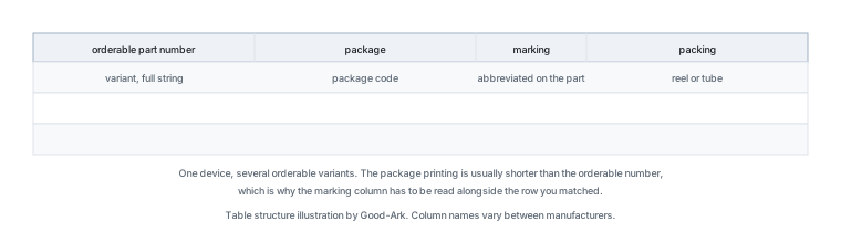
If the complete number is not in the table, the useful conclusion is that you do not have a valid orderable variant, rather than that you have an unusual one. Three explanations are common: the listing abbreviated the number, the part is a different family whose prefix you misread, or the part is not what it claims to be. In the first case the full number from the package resolves it; in the second, checking the family page does; and in the third, no amount of decoding will help, which is why our article on sourcing and verification exists.
Decoder worksheet
The routine, in five steps, for any unfamiliar part number.
- Read the complete number from the package, including any suffix, and note any manufacturer mark.
- Find the manufacturer’s family page for that prefix.
- Open the current datasheet and find the ordering-information table.
- Match the full number, not a truncated version of it.
- Check the marking specification to confirm your package’s printing matches the row you matched.
Related reading on our own site covers cataloguing conventions: part numbers and electronic components, and the barcode meaning of the same letters is described under GS1. Component test methods come from JEDEC, marking and traceability expectations in production from IPC, the documentation duties that keep a revision traceable from ISO, and sector-level context from the Semiconductor Industry Association. Device and quality background is published by NIST and IEC.
What Are the Most Important GS Prefix Selection Takeaways?
The GS prefix helps identify a Good-Ark Electronics semiconductor family, but the full datasheet determines whether a specific device fits the application. Select parts using voltage margin, hot on-resistance, gate-drive compatibility, switching behavior, package thermal capability, and qualification requirements.
Actionable selection advice is straightforward:
-
Define worst-case voltage, current, temperature, and switching-frequency conditions before searching for parts.
-
Use RDS(on)R_{DS(on)} at the intended gate-drive voltage and elevated junction temperature.
-
Include transient voltage, ringing, avalanche, inrush, and fault conditions in the voltage-margin plan.
-
Treat gate threshold voltage as a turn-on reference, not a full-enhancement guarantee.
-
Validate PCB layout, gate resistance, thermal spreading, and EMI performance with hardware testing.
-
Confirm exact product documentation and qualification status before production release.
What is the difference between GS and VGSV_{GS}? GS is commonly part of a Good-Ark Electronics product designation, while VGSV_{GS} is the electrical voltage measured from a MOSFET gate to its source.
Does a GS prefix identify an N-channel MOSFET? Not necessarily. The prefix alone does not reliably define channel type. Confirm polarity, voltage rating, and package using the complete part number and datasheet.
Can I select a MOSFET using only its current rating? No. Current rating must be reviewed with voltage, thermal resistance, on-resistance, switching loss, safe operating area, PCB cooling, and operating temperature.
Why is a low RDS(on)R_{DS(on)} MOSFET not always the best choice? A lower resistance may come with higher gate charge, different switching loss, a larger package, or higher cost. The best device minimizes total system loss and risk.
How can I confirm a MOSFET is fully enhanced? Check the datasheet’s guaranteed RDS(on)R_{DS(on)} values and their stated VGSV_{GS} test conditions. Drive the gate at a supported voltage and validate it under real load and temperature.
FAQs
Does a GS prefix in a MOSFET part number mean anything electrical?
It identifies the family or series the device belongs to. Everything that matters electrically, such as breakdown voltage, on-resistance, gate charge, and thermal resistance, still has to be read from the datasheet for that exact ordering code.
Which current rating should I design to?
The one that matches your thermal path. A case-referenced rating assumes an ideal heat sink, while an ambient-referenced rating assumes a specific copper area in still air. Calculate the junction temperature your board will produce, then compare against the derated limit.
My gate driver is 3.3 V. Can I use a device specified at 10 V?
Not on the strength of the 10 V on-resistance figure. You need a guaranteed resistance value at your gate voltage, or a driver that produces the specified gate voltage. A threshold voltage only tells you where the device begins to conduct, not where it is fully enhanced.
How do I check that a MOSFET survives a fault?
Use the safe operating area chart for the pulse width your circuit will see, together with the thermal impedance curve, rather than the single-pulse avalanche or pulsed-current ratings alone. Those headline numbers describe one event, not repeated stress.
Related Articles
Official Resources
References
- All About Circuits – Insulated-Gate Field-Effect Transistors (MOSFET)
- JEDEC JESD24 – Power MOSFET test methods and measurement conditions
- Semiconductor Engineering – System-Level Electro-Thermal Analysis of RDS(on) for Power MOSFETs
- Power Electronics News – AOS Launches alphaMOS E2 600V Super Junction MOSFET
- Semiconductor Engineering – Safe and Reliable MOSFET Operation in Bidirectional Power Switches
Continue through this engineering topic
For the complete selection, design, verification, and troubleshooting path, explore the Good-Ark Product and Sourcing Hub.
Recommended
 Why Do Diodes Get Hot? Conduction and Switching Losses ExplainedInfoStandard, Fast Recovery, and Schottky Diodes: What’s the Difference?Info
 What Is a Fast Recovery Diode? Understanding “Fast Recovery”Info
 What Is a Diode? A Beginner’s Guide to How It WorksInfo
 Automotive Semiconductor Report 2026: Chips Per Car Keep RisingKnowledge