Switching Mode Power Supply: Component Selection and Project Validation
Updated: October 28, 2026 A switching mode power supply (SMPS) only meets its efficiency, thermal, and EMI targets when the discrete parts…
Updated: October 28, 2026
A switching mode power supply (SMPS) only meets its efficiency, thermal, and EMI targets when the discrete parts around the controller are chosen for the actual waveform—and then proven on the bench. This guide focuses on component selection by power-stage role and on a practical project-validation sequence, not on buying a finished AC-DC brick.
What “component selection” means for an SMPS
Component selection for an SMPS means matching semiconductors and passives to voltage, current, temperature, and switching events in each stage—not copying a reference BOM blindly.
Controllers and magnetics set the architecture, but diodes, MOSFETs, snubbers, and surge parts often decide whether the design survives first-article testing. Treat each power-stage role as its own shortlist problem with explicit operating points.
If you need a refresher on how an SMPS converts and regulates power, start with the site’s switching power supply overview, then return here for selection and validation. Manufacturer primers such as Analog Devices’ SMPS basics and Tektronix’s switching supply guide are useful for topology language; they do not replace a stage-level parts checklist.
Map the power stages before you open a catalog
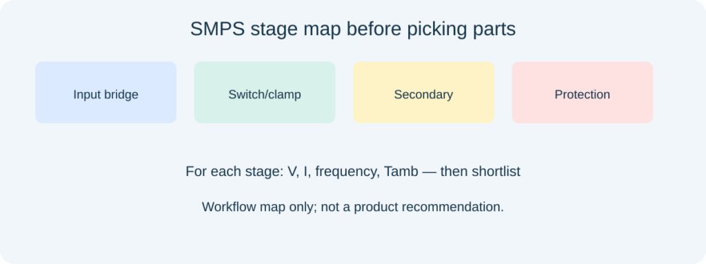
List the stages that actually appear in your schematic: AC input rectifier or DC front end, optional PFC, primary switch network, clamp or snubber, secondary rectifier, and output protection. For each stage write peak voltage, average and peak current, switching or line frequency, and the hottest ambient you must support.
That map prevents common mistakes—such as ranking Schottky rectifiers only by cold forward voltage, or picking a MOSFET by RDS(on) alone while ignoring gate charge and body-diode recovery in a hard-switched bridge. Keep the map in the design file so sourcing and validation use the same numbers.
| Stage | Typical semiconductor focus | First checks |
|---|---|---|
| Input bridge / front-end rectifier | Si rectifier or bridge module | VRRM, IF(AV), surge, thermal path |
| Primary switch | Si MOSFET (or other switch technology as designed) | VDSS, RDS(on) at hot, Qg, SOA |
| Clamp / snubber diode | Fast / ultrafast or controlled-recovery diode | Reverse recovery, voltage margin, package inductance |
| Secondary rectifier | Schottky or fast recovery, Si or SiC as required | VR, VF/IR at temperature, pulsed current |
| Protection | TVS, Zener, or dedicated protection diode | Clamp level, energy, unidirectional vs bidirectional |
How do you select the input rectifier for a switching mode power supply?
Size voltage and surge first, then thermal rise at the average current you actually draw.
Peak line and DC-bus voltage set the reverse rating with margin; inrush and hold-up events set the surge rating. Average current alone is not enough if the bridge shares a small heatsink with other losses.
For discrete bridges versus modules, confirm pinout, isolation of the package tab if present, and whether the datasheet thermal resistance assumes a defined copper area or an external heatsink. The power rectifier selection guide covers rating definitions that also apply at the SMPS front end.
Primary switch and clamp: what to compare on the datasheet
Compare MOSFET candidates at the same junction temperature and the same gate drive you can deliver. A low RDS(on) figure measured at a strong gate voltage is not usable if your driver cannot reach that condition under load. Gate charge and switching energy matter as frequency rises; body-diode behavior matters in topologies that force diode conduction.
Clamp and snubber diodes must survive the voltage spike they are meant to catch. Prefer parts with documented reverse-recovery or softness characteristics that match the layout inductance you measured or simulated. Do not treat a generic “fast diode” label as a substitute for those curves.

Secondary rectifier: efficiency versus leakage and stress
Secondary rectifiers often dominate conduction loss at low output voltage. Schottky options can reduce forward drop, but reverse leakage rises with temperature and can reorder the ranking. Compare VF and IR at the same current, reverse voltage, and hot temperature—not at mismatched catalog highlights. See the Schottky selection guide for that trade-off in more detail.
When reverse voltage or temperature push silicon Schottky outside a comfortable window, evaluate fast-recovery silicon or wide-bandgap rectifiers using the same waveform assumptions. Package thermal resistance on the intended copper must support the calculated loss.
Protection parts that belong in the first shortlist
Place surge and clamp devices where the energy actually appears: input lines, DC bus, or sensitive nodes after the secondary. A Zener used as a light clamp is not interchangeable with a TVS sized for repetitive or high-energy transients. Keep unidirectional versus bidirectional polarity consistent with the circuit. The protection diodes overview helps separate those roles.
Project validation: prove the shortlist on hardware
Validation means measuring the operating points you used for selection, then stressing the corners the datasheet already warns about.
- Bring-up: verify input voltage range, soft-start, and no abnormal FET or diode heating at no load and light load.
- Efficiency and loss: record efficiency at defined loads; infrared or thermocouple checks on rectifiers and switches at the hottest expected ambient.
- Waveforms: capture switch-node and secondary rectifier voltage for overshoot against device ratings with margin.
- Startup and step load: confirm output stays within regulation and that surge parts are not repeatedly avalanching.
- EMI smoke check: even a pre-compliance scan can reveal snubber or layout issues before certification.
Document the exact firmware/hardware revision with each dataset. If a part change is proposed for cost or availability, repeat the thermal and overshoot checks—do not assume electrical equivalence from a similar catalog title.

Passives and layout that change semiconductor stress
Inductor and transformer leakage, PCB loop area, and snubber RC values change the voltage the clamp diode and MOSFET actually see. A part that looked fine in a spreadsheet can avalanche every cycle if the layout inductance is higher than the reference design. When you shortlist semiconductors, freeze the intended layout rules—Kelvin sense for current, gate-return path, and copper under power packages—or validation will fight a moving target.
Input bulk capacitance and hold-up time also set inrush and ripple current through the front-end rectifier. If you raise capacitance for longer hold-up, revisit surge ratings and NTC or active inrush methods together with the bridge shortlist.
A practical selection-and-validation worksheet
Keep one worksheet per power stage with columns for required V/I/T, candidate A/B, datasheet condition notes, measured overshoot, measured temperature, and pass/fail. Require two signatures for any second-source add: design owner and test owner. That discipline is what separates a durable SMPS program from a BOM that only worked on the first spin.
Arrow and other industry articles emphasize efficiency and EMI as system outcomes of switching behavior; treat those outcomes as validation gates after the stage map is filled, not as slogans that replace ratings. For a worked build-oriented view of SMPS blocks, Circuit Basics’ switched-mode supply article shows how stages connect—use it for intuition, then apply your own electrical limits.
Where Good-Ark’s public product scope fits this workflow
Good-Ark (Suzhou Good-Ark Electronics) publicly lists rectifier diodes, Schottky devices, Zener diodes, bridge products, and related discrete lines on en.goodark.com, with SMPS called out among application areas on the company’s application pages. Use those pages and datasheets to verify package and ratings for a shortlisted role—never as a substitute for measuring your own bus voltage and thermal rise.
Frequently asked questions
Is an SMPS always more efficient than a linear supply?
Often at higher step-down ratios and loads, but not automatically at every light-load or noise-sensitive point. Compare measured efficiency and EMI for your load profile.
Can I validate an SMPS with datasheet typical values only?
No. Typical curves help shortlist candidates; project validation must use your layout, drive strength, and ambient extremes.
What is the first measurement after a rectifier substitution?
Confirm reverse voltage margin on the waveform and the new part’s steady temperature at full load before closing the change.
Do I need SiC parts for every modern SMPS?
No. Silicon MOSFETs and silicon rectifiers remain appropriate in many voltage and cost envelopes; wide-bandgap parts help when voltage, frequency, or loss targets demand them.
Continue through this engineering topic
- What is a switching power supply?
- How to choose the right power rectifier
- Schottky barrier rectifier practical selection
- Protection diodes overview
Topic hub: What is a switching power supply — related SMPS and rectifier guides in this cluster.
Recommended
 How to Test a Diode in Circuit: Readings You Can and Cannot TrustKnowledge
 How to Check Diode Positive and Negative When the Band Is WornKnowledge
 Diode Symbol Explained: Schematic Marks vs the Package You HoldKnowledgeGaN Traction Inverters Reach Vehicle Demonstrators: Status Check vs SiC MainstreamKnowledgeSiC Wafer Price Drops Explained: When Silicon Carbide Beats Silicon for Real DesignsKnowledge
 Diode Polarity: Anode, Cathode, Stripe Marks, and How Not to Reverse ItKnowledge