Inside a Diode Factory: How Diodes Are Manufactured, Explained Without Jargon
How are diodes manufactured? Eight steps from a crystal of silicon to a taped reel, the questions each step raises, and where quality is won or lost.
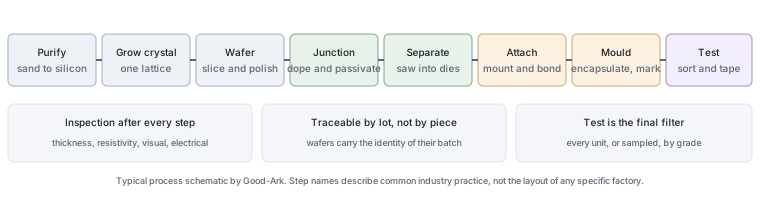
Most explanations of diodes start with the junction and stop there, which leaves out the part that determines whether the part in your hand behaves like the one in the datasheet. The junction is a few micrometres thick; everything around it — the crystal, the package, the wire and the test — is what a factory actually does all day. Here is that process, in the order it happens, with the question an engineer would ask at each stage.
Last updated:
Start with sand: where silicon comes from
Silicon is the second most abundant element in the Earth’s crust, and it usually starts its industrial life as quartz sand. The sand is reduced in a furnace with carbon to give metallurgical-grade silicon, which is then purified chemically until the remaining impurities are measured in parts per billion. Purification is where the cost begins, because it takes a lot of energy to move a material from 98 per cent pure to something a semiconductor process can accept.
The analogy worth holding on to is that of making a perfect ice cube. What matters is not the water but the absence of anything else in it, and in a crystal, “anything else” means individual atoms of boron, phosphorus or metal sitting where silicon should be. At the concentrations involved, a stray atom in a billion is a design feature; a stray atom in a million is a defect.
Growing a crystal
The purified silicon is melted and a seed crystal is dipped into it, then slowly withdrawn while rotating. The molten silicon solidifies onto the seed in a continuous single crystal, forming a cylindrical ingot typically a metre or more long. Because the ingot is one continuous lattice rather than a mass of grains, current can cross it predictably, which is the whole point.
The growth recipe already decides part of the final device. Dopant atoms are added to the melt to set the background resistivity, and the pulling rate and temperature gradient affect how uniformly those dopants distribute. A factory can therefore make wafers with different starting characteristics from the same line, which is one reason a component datasheet lists a range rather than a single number.
Cutting wafers and building the junction
The ingot is sliced into thin wafers, each polished until its surface is flat to a fraction of a micrometre. Into that surface, the manufacturer introduces dopant atoms in a pattern: a region with excess electrons, a region with a deficit, and a boundary between them. That boundary is the junction, and it is what makes the device conduct in one direction and block in the other.
For a rectifier, the junction is usually not a delicate surface structure but a deep, robust one, because the device has to survive reverse voltage and surges. After the junction forms, the surface is passivated — covered with a stable layer that stops contaminants and moisture from reaching the boundary — and metal contacts are deposited on both faces. Passivation is unglamorous and decisive: a great junction with a poor surface becomes a device that leaks.
Sawing dies and mounting them
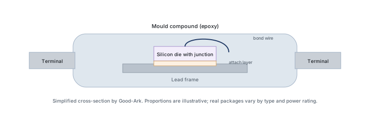
A finished wafer carries hundreds or thousands of identical devices. It is thinned, mounted on film and cut along streets between the devices, producing individual dies. Each die is then attached to its package: to a lead frame in a plastic part, or to a metal base in a stud or press-fit package where heat has to leave through the bottom. The attach material matters as much as the die, because it is part of the thermal path and part of the electrical connection.
This is the first stage where a customer’s use case changes the process. A part destined for a sealed automotive module and a part destined for an open-frame power supply may start from the same wafer and diverge here, in attach material, lead frame and package.
Wire bonding and moulding
Electrical connections are made from the die surface to the package terminals: fine aluminium or gold wires in small devices, heavier ribbons or clips in power devices, where current is high and every milliohm counts. Then the assembly is encapsulated in epoxy, cured, and the terminals are plated so they can be soldered reliably at the customer’s factory.
Moulding looks like a packaging step and behaves like an electrical one. The mould compound provides mechanical protection, electrical insulation and part of the moisture barrier, and its thermal expansion has to be close enough to the metal inside that temperature cycling does not tear the assembly apart. Most field failures in plastic packages, when they are not electrical, are mechanical failures of exactly this interface.
Testing, marking and taping
Every unit is then tested electrically: forward voltage, reverse leakage, breakdown voltage and, for switching devices, the timing parameters. Parts are sorted into grades against the specification, and out-of-spec units are scrapped or downgraded. After test the device is marked — with the part number, and with a lot or date code that ties it back to the wafer batch and the process it went through — and packed into tubes or tape and reel for automated assembly.
That lot code is the reason process control matters commercially. It is the only link between the device in a customer’s product and the conditions it was made under, and it is what makes an investigation possible when something goes wrong two years later.
| Stage | What can go wrong | How it appears afterwards |
|---|---|---|
| Crystal growth and wafering | Resistivity drift, surface damage | Parts that sit outside the datasheet curve |
| Junction formation and passivation | Contamination, weak surface layer | Reverse leakage that climbs with temperature and humidity |
| Die attach and bonding | Voids, weak interface, poor thermal path | Overheating under load and early thermal fatigue |
| Moulding and plating | Delamination, solderability problems | Assembly defects and moisture-related failures |
| Test and sorting | Sampling instead of full screening, loose limits | Out-of-spec parts reaching a production line |
| Marking and packing | Lost lot identity, mixed parts in a reel | No traceability when a batch misbehaves |
Where quality can be lost
Three stages account for a large share of the difference between a good and a mediocre supplier. The first is surface passivation and contamination control, because a leaky device is almost always a surface problem rather than a bulk one. The second is the attach and bond interface, where voids, delamination or a poor thermal path show up as overheating under load rather than as an immediate failure. The third is test coverage: whether the supplier screens every unit or samples, and how the test limits are set relative to the datasheet.
None of this is visible from the outside of a finished part, which is why buyers rely on process evidence — audit reports, qualification data, lot traceability and change notification — rather than on inspection alone. Our article on what to verify before mass production turns those points into a checklist.
If you want to check a supplier’s process claims against something external, the reference points are public: JEDEC for discrete device test methods, ISO for the quality management systems that audit reports refer to, and IPC for assembly and inspection expectations. The device behaviour that the process exists to protect is summarised in our explainer on diodes, and the wider industry context is reported by the Semiconductor Industry Association. Sector and quality background is published by NIST and IEC.
How to explain this in one minute
Sand becomes extremely pure silicon. The silicon is grown into a single crystal, sliced into wafers and doped so that a boundary forms between two differently treated regions. Each device on the wafer is cut out, mounted in a package, connected by wire or clip and sealed in epoxy. Then it is tested, marked with a code that identifies its batch, and taped for a machine to place on a board. Everything the datasheet promises was decided somewhere in those steps, not at the moment you switch the circuit on.
FAQ
What kills diodes?
In rough order of how often they appear: excessive forward current that overheats the junction, a reverse voltage beyond the rating, a surge that exceeds the device’s non-repetitive capability, and thermal fatigue from repeated heating and cooling. Manufacturing defects exist, but a failed diode is far more often an application problem — a wrong rating, a missing heatsink, or a transient the design never accounted for.
Are diodes still used today?
Constantly, and in larger numbers than most people expect. Almost anything that plugs into a wall socket rectifies AC to DC at some point, and every device with a battery needs protection against reverse connection or surge. Since 1990 the manufacturer described on this site has built its portfolio around those devices, and the volumes keep rising as more products become electronic.
Do diodes use AC or DC?
Both, in different roles. A rectifier diode is designed to take alternating current in and deliver a pulsing direct current out, which is why rectifiers sit at the input of a power supply. Elsewhere, in a signal path or a protection circuit, a diode usually works with direct current and exists to block one direction or clamp a voltage. The device does not care about the label — it responds to the instantaneous voltage across it.
How is a diode constructed?
A silicon crystal is doped so that one region has surplus electrons and an adjacent region has a deficit, creating a junction that conducts in one direction. Metal contacts are added on both faces, the surface is passivated, the die is mounted on a lead frame or base, connected with wire or clip, and encapsulated in mould compound. The final part is tested, marked and packed. Every one of those steps is described above in more detail.
Why does the lot code on the package matter?
It is the only link between the part in your product and the conditions it was manufactured under. If a batch behaves differently from the sample you qualified, the lot code is what allows the manufacturer to trace the wafer, the process settings and the test data. Without it, an investigation has nowhere to start.
What to do next
The practical use of this article is not to memorise the process but to know where to ask questions. If a supplier cannot explain how the junction surface is passivated, how the die is attached, or how test limits are set, that is information about the supplier — and it is obtainable in one conversation.
Good-Ark can explain how a device family is built, provide the qualification documentation that applies to it, and confirm the traceability available with a shipment. Write to sales@goodark.com, or start with the quality knowledge section.
This article is published by Good-Ark, a manufacturer described in it. The process description is typical industry practice; it is not a specification of any particular plant, and no capacity, yield or equipment claims are made.
Continue reading
Browse the Good-Ark Product and Sourcing Hub for related guides.
Recommended
 Why Do Diodes Get Hot? Conduction and Switching Losses ExplainedInfoStandard, Fast Recovery, and Schottky Diodes: What’s the Difference?Info
 What Is a Fast Recovery Diode? Understanding “Fast Recovery”Info
 What Is a Diode? A Beginner’s Guide to How It WorksInfo
 Automotive Semiconductor Report 2026: Chips Per Car Keep RisingKnowledge